Heavy output current loads, Layout and grounding – Rainbow Electronics MAX829 User Manual
Page 7

MAX828/MAX829
Switched-Capacitor Voltage Inverters
_______________________________________________________________________________________
7
Heavy Output Current Loads
When under heavy loads, where higher supply is sourcing
current into OUT, the OUT supply must not be pulled
above ground. Applications that sink heavy current into
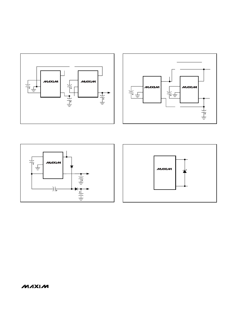
OUT require a Schottky diode (1N5817) between GND
and OUT, with the anode connected to OUT (Figure 7).
Layout and Grounding
Good layout is important, primarily for good noise perfor-
mance. To ensure good layout, mount all components as
close together as possible, keep traces short to mini-
mize parasitic inductance and capacitance, and use a
ground plane.
Shutting Down the MAX828/MAX829
For a similar device with logic-controlled shutdown,
please refer to the MAX1719/MAX1720/MAX1721. To
add manual shutdown control to the MAX828/MAX829,
use the circuit in Figure 8. The output resistance of the
MAX828/MAX829 will typically be 20
Ω plus two times
the output resistance of the buffer driving IN. The 0.1µF
capacitor at the IN pin absorbs the transient input cur-
rents of the MAX828/MAX829.
The output resistance of the buffer driving the IN pin can
be reduced by connecting multiple buffers in parallel.
The polarity of the SHUTDOWN signal can also be
changed by using a noninverting buffer to drive IN.
MAX828
MAX829
“n”
MAX828
MAX829
“1”
2
1
V
OUT
C2
2
+V
IN
C1
C2
C1
3
3
4
4
5
5
1
V
OUT
= -nV
IN
…
…
Figure 4. Cascading MAX828s or MAX829s to Increase
Output Voltage
MAX828
MAX829
“n”
MAX828
MAX829
“1”
2
1
V
OUT
C2
2
+V
IN
C1
C1
3
3
4
4
5
5
1
V
OUT
= -V
IN
R
OUT
=
R
OUT
OF SINGLE DEVICE
NUMBER OF DEVICES
…
…
Figure 5. Paralleling MAX828s or MAX829s to Reduce Output
Resistance
MAX828
MAX829
2
1
V
OUT
= (2V
IN
) -
(V
FD1
) - (V
FD2
)
C2
+V
IN
C1
3
4
5
V
OUT
= -V
IN
C4
D1
D1, D2 = 1N4148
C3
D2
Figure 6. Combined Doubler and Inverter
MAX828
MAX829
4
1
GND
OUT
Figure 7. High V- Load Current
