Detailed description, Applications information – Rainbow Electronics MAX829 User Manual
Page 5
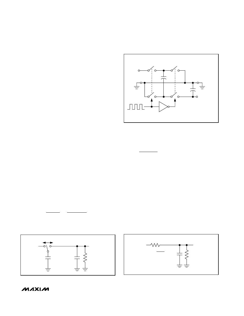
_______________Detailed Description
The MAX828/MAX829 capacitive charge pumps invert the
voltage applied to their input. For highest performance,
use low equivalent series resistance (ESR) capacitors.
During the first half-cycle, switches S2 and S4 open,
switches S1 and S3 close, and capacitor C1 charges to
the voltage at IN (Figure 2). During the second half-
cycle, S1 and S3 open, S2 and S4 close, and C1 is level
shifted downward by V
IN
volts. This connects C1 in par-
allel with the reservoir capacitor C2. If the voltage across
C2 is smaller than the voltage across C1, then charge
flows from C1 to C2 until the voltage across C2 reaches -
V
IN
. The actual voltage at the output is more positive
than -V
IN
, since switches S1–S4 have resistance and the
load drains charge from C2.
Charge-Pump Output
The MAX828/MAX829 are not voltage regulators: the
charge pump’s output source resistance is approxi-
mately 20
Ω at room temperature (with V
IN
= +5V), and
V
OUT
approaches -5V when lightly loaded. V
OUT
will
droop toward GND as load current increases. The
droop of the negative supply (V
DROOP-
) equals the cur-
rent draw from OUT (I
OUT
) times the negative convert-
er’s source resistance (RS-):
V
DROOP-
= I
OUT
x RS-
The negative output voltage will be:
V
OUT
= -(V
IN
- V
DROOP-
)
Efficiency Considerations
The efficiency of the MAX828/MAX829 is dominated by
its quiescent supply current (I
Q
) at low output current
and by its output impedance (R
OUT
) at higher output
current; it is given by:
where the output impedance is roughly approximated
by:
The first term is the effective resistance of an ideal
switched-capacitor circuit (Figures 3a and 3b), and
R
SW
is the sum of the charge pump’s internal switch
resistances (typically 8
Ω to 9Ω at V
IN
= +5V). The typical
output impedance is more accurately determined from
the Typical Operating Characteristics.
Applications Information
Capacitor Selection
To maintain the lowest output resistance, use capacitors
with low ESR (Table 1). The charge-pump output resis-
tance is a function of C1’s and C2’s ESR. Therefore,
minimizing the charge-pump capacitor’s ESR minimizes
the total output resistance.
R
1
f
x C1
2R
4ESR
ESR
OUT
OSC
SW
C1
C2
≅
( )
+
+
+
I
I
I
1
I
x R
V
OUT
OUT
Q
OUT
OUT
IN
η ≅
+
−
MAX828/MAX829
Switched-Capacitor Voltage Inverters
_______________________________________________________________________________________
5
S1
IN
S2
S3
S4
C1
C2
V
OUT
= -(V
IN
)
Figure 2. Ideal Voltage Inverter
V+
C1
f
C2
R
L
V
OUT
Figure 3a. Switched-Capacitor Model
R
EQUIV
=
R
EQUIV
V
OUT
R
L
1
V+
f
× C1
C2
Figure 3b. Equivalent Circuit