Max1197, Applications information – Rainbow Electronics MAX1197 User Manual
Page 14
MAX1197
where f
IN
represents the analog input frequency and
t
AJ
is the time of the aperture jitter.
Clock jitter is especially critical for undersampling
applications. The clock input should always be consid-
ered as an analog input and routed away from any ana-
log input or other digital signal lines.
The MAX1197 clock input operates with a voltage thresh-
old set to V
DD
/2. Clock inputs with a duty cycle other
than 50% must meet the specifications for high and low
periods as stated in the Electrical Characteristics table.
System Timing Requirements
Figure 3 depicts the relationship between the clock
input, analog input, and data output. The MAX1197
samples at the rising edge of the input clock. Output
data for channels A and B is valid on the next rising
edge of the input clock. The output data has an internal
latency of five clock cycles. Figure 3 also determines
the relationship between the input clock parameters
and the valid output data on channels A and B.
Digital Output Data (D0A/B–D7A/B), Output
Data Format Selection (T/B), Output
Enable (OE)
All digital outputs, D0A–D7A (channel A) and D0B–D7B
(channel B), are TTL/CMOS-logic compatible. There is a
five-clock-cycle latency between any particular sample
and its corresponding output data. The output coding
can either be straight offset binary or two’s complement
(Table 1) controlled by a single pin (T/B). Pull T/B low to
select offset binary and high to activate two’s comple-
ment output coding. The capacitive load on the digital
outputs D0A–D7A and D0B–D7B should be kept as low
as possible (<15pF), to avoid large digital currents that
could feed back into the analog portion of the MAX1197,
thereby degrading its dynamic performance. Using
buffers on the digital outputs of the ADCs can further
isolate the digital outputs from heavy capacitive loads.
To further improve the dynamic performance of the
MAX1197, small series resistors (e.g., 100
Ω) may be
added to the digital output paths close to the MAX1197.
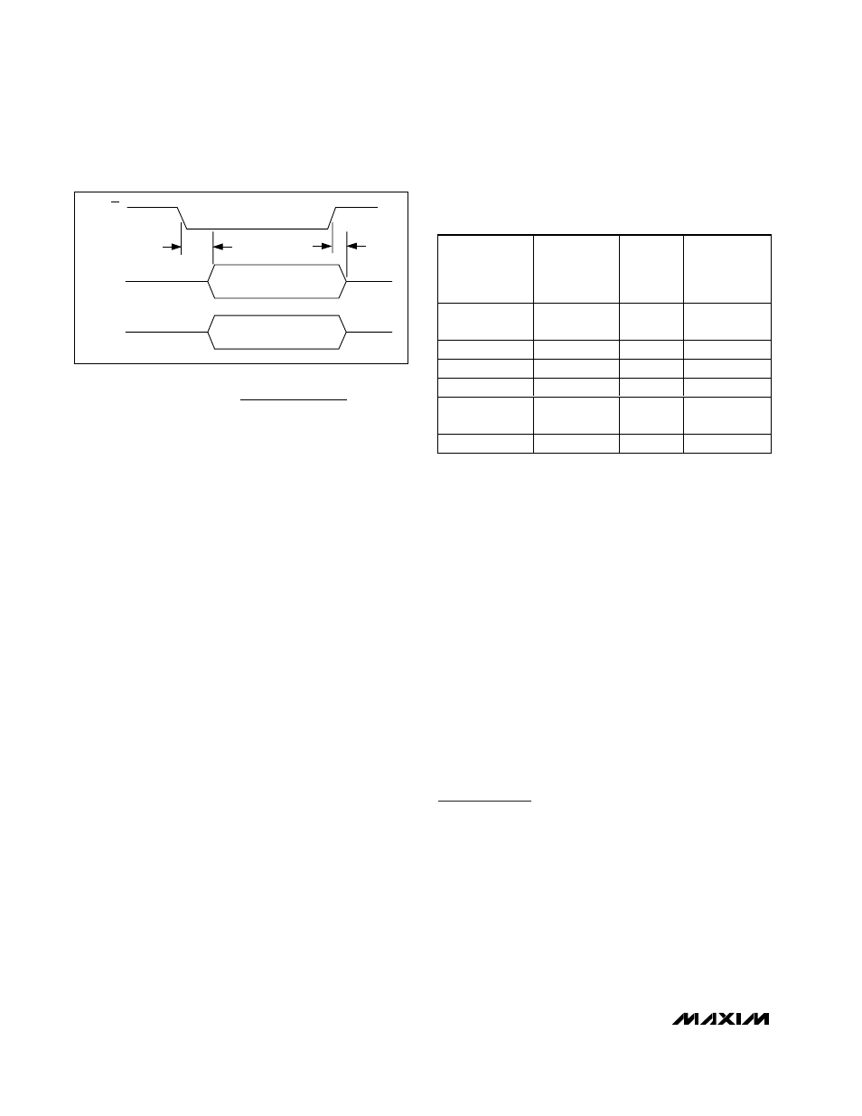
Figure 4 displays the timing relationship between out-
put enable and data output valid, as well as power-
down/wake-up and data output valid.
Power-Down and Sleep Modes
The MAX1197 offers two power-save modes—sleep
mode (SLEEP) and full power-down (PD) mode. In
sleep mode (SLEEP = 1), only the reference bias circuit
is active (both ADCs are disabled), and current con-
sumption is reduced to 3mA.
To enter full power-down mode, pull PD high. With OE
simultaneously low, all outputs are latched at the last
value prior to the power down. Pulling OE high forces
the digital outputs into a high-impedance state.
Applications Information
Figure 5 depicts a typical application circuit containing
two single-ended-to-differential converters. The internal
reference provides a V
DD
/2 output voltage for level-
shifting purposes. The input is buffered and then split
to a voltage follower and inverter. One lowpass filter per
amplifier suppresses some of the wideband noise
associated with high-speed operational amplifiers. The
user can select the R
ISO
and C
IN
values to optimize the
filter performance, to suit a particular application. For
the application in Figure 5, a R
ISO
of 50
Ω is placed
before the capacitive load to prevent ringing and oscil-
SNR
f
t
IN
AJ
log
=
Ч
Ч
Ч
Ч
20
1
2
π
Dual, 8-Bit, 60Msps, 3V, Low-Power ADC with
Internal Reference and Parallel Outputs
14
______________________________________________________________________________________
OUTPUT
D7A–D0A
OE
t
DISABLE
t
ENABLE
HIGH-Z
HIGH-Z
VALID DATA
OUTPUT
D7B–D0B
HIGH-Z
HIGH-Z
VALID DATA
Figure 4. Output Timing Diagram
ST RA IG HT
O F FSET
B INA R Y
T WO’S
C O M PL EM EN T
D IFF ER EN T IAL
IN PU T
VO LT A G E*
D IFF ER EN T IAL
IN PU T
T/B = 0
T/B = 1
V
REF
x 255/256
+Full Scale
-1LSB
1111 1111
0111 1111
V
REF
x 1/256
+1LSB
1000 0001
0000 0001
0
Bipolar zero
1000 0000
0000 0000
-V
REF
x 1/256
-1LSB
0111 1111
1111 1111
-V
REF
x 255/256
-Full Scale
+1LSB
0000 0001
1000 0001
-V
REF
x 256/256
-Full Scale
0000 0000
1000 0000
Table 1. MAX1197 Output Codes For
Differential Inputs
*V
REF
= V
REFP
- V
REFN