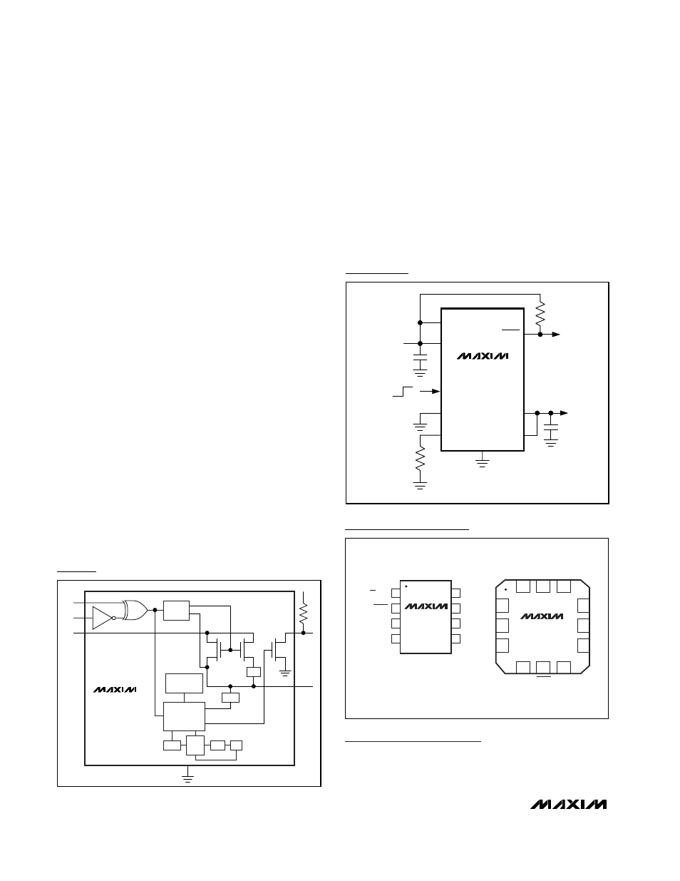
Chip information, Typical application circuit, Max1563 functional diagram – Rainbow Electronics MAX1563 User Manual
Page 10: Pin configurations, X (v, Transistor count: 1833 process: bicmos

MAX1562/MAX1562H/MAX1563
Layout and Thermal Dissipation
Keep all traces as short as possible to reduce the effect
of undesirable parasitic inductance and optimize the
switch response time to output short-circuit conditions.
Place the input and output capacitors no more than
5mm from the device leads. Connect IN and OUT to the
power bus with short traces. Wide power bus planes at
IN and OUT provide superior heat dissipation.
Calculate the power dissipation for a normal loaded
condition as follows:
P = (I
OUT
)
2
x R
ON
At a 3A operating current and the maximum on-resis-
tance of the switch (50m
Ω), the power dissipation is:
P = (3A)
2
x 0.05
Ω = 450mW
The worst-case power dissipation occurs when the out-
put current is just below the current-limit threshold (set
to 3A in this example) with an output voltage greater
than +1V. In this case, the power dissipated in the
switch is the voltage drop across the switch multiplied
by the current limit:
P = I
LIM
x (V
IN
- V
OUT
)
For a +5V input and +1V output, the maximum power
dissipation is:
P = 3A x (5V - 1V) = 12W
Because the package power dissipation is 471mW for
the MAX1562/MAX1562H and 1.35W for the MAX1563,
the devices’ die temperature exceeds the +160°C ther-
mal-shutdown threshold, and the switch output shuts
down until the junction temperature cools by 15°C. The
duty cycle and period are strong functions of the ambi-
ent temperature and the PC board layout.
If the output current exceeds the current-limit threshold,
or the output voltage is pulled below the short-circuit
detect threshold, the MAX1562/MAX1562H/MAX1563
enter a fault state for 20ms, after which autoreset mode
is enabled and 25mA is sourced by the output. For a
+5V input, OUT short-circuited to GND, and autoreset
mode active, the power dissipation is as follows:
P = 0.025A x 5V = 0.125W
Chip Information
TRANSISTOR COUNT: 1833
PROCESS: BiCMOS
Programmable 4A USB Current-Limited
Switches with Autoreset and Fault Blanking
10
______________________________________________________________________________________
MAX1563
FAULT
OUT
OUT
ISET
SEL
ON
IN
IN
USB
PORT
GND
INPUT
+4V TO +5.5V
OFF
ON
1
µF
4.7
µF*
100k
Ω
*USB APPLICATIONS MAY REQUIRE
ADDITIONAL BULK CAPACITANCE.
Typical Application Circuit
CHARGE
PUMP
THERMAL
SHUTDOWN
FAULT LOGIC
20ms TIMERS
ILIM
25mA
ULVO
OSC
25kHz
REF
BIAS
ON
SEL
IN
MAX1563
OUT
GND
FAULT
IN
MAX1563 Functional Diagram
TOP VIEW
() FOR MAX1562H.
OUT
IN
ISET
1
2
8
7
OUT
IN
FAULT
GND
ON (ON)
SO
3
4
6
5
MAX1562
MAX1562H
12
IN
11
N.C.
10
OUT
9
IN
8
N.C.
7
ISET
4
ON
5
FAULT
6
GND
1
OUT
2
N.C.
3
SEL
MAX1563
QFN
Pin Configurations
