Design procedure – Rainbow Electronics MAX859 User Manual
Page 8

MAX856–MAX859
3.3V/5V or Adjustable-Output,
Step-Up DC-DC Converters
8
_______________________________________________________________________________________
Logic Inputs and Outputs
The 3/5 input is internally diode clamped
to GND
and
OUT, and should not be connected to signals outside
this range. The SHDN input and LBO output (open-
drain) are not clamped to V+ and can be pulled as high
as 7V regardless of the voltage at OUT
.
Do not leave
control inputs (3/5, LBI, or SHDN) floating.
__________________Design Procedure
Output Voltage Selection
For the MAX856/MAX858,you can select a 3.3V or 5V
output voltage under logic control, or by tying 3/
–
5 to
GND or OUT. Efficiency is typically better than 80%
over a 2mA to 100mA (MAX856/MAX857) load range.
The device is internally bootstrapped, with power
derived from the output voltage (via OUT). When the
output is in 5V mode, the higher internal supply voltage
results in lower switch-transistor on-resistance, slightly
greater output power, and higher efficiency.
Bootstrapping allows the battery voltage to sag to 0.8V
once the system is started. Therefore, the battery volt-
age ranges from (V
OUT
+ V
D
) to 0.8V (where V
D
is the
forward drop of the Schottky rectifier). If the battery volt-
age exceeds the programmed output voltage, the out-
put will follow the battery voltage. This is acceptable in
many systems; however, the input or output voltage
must not be forced above 7V.
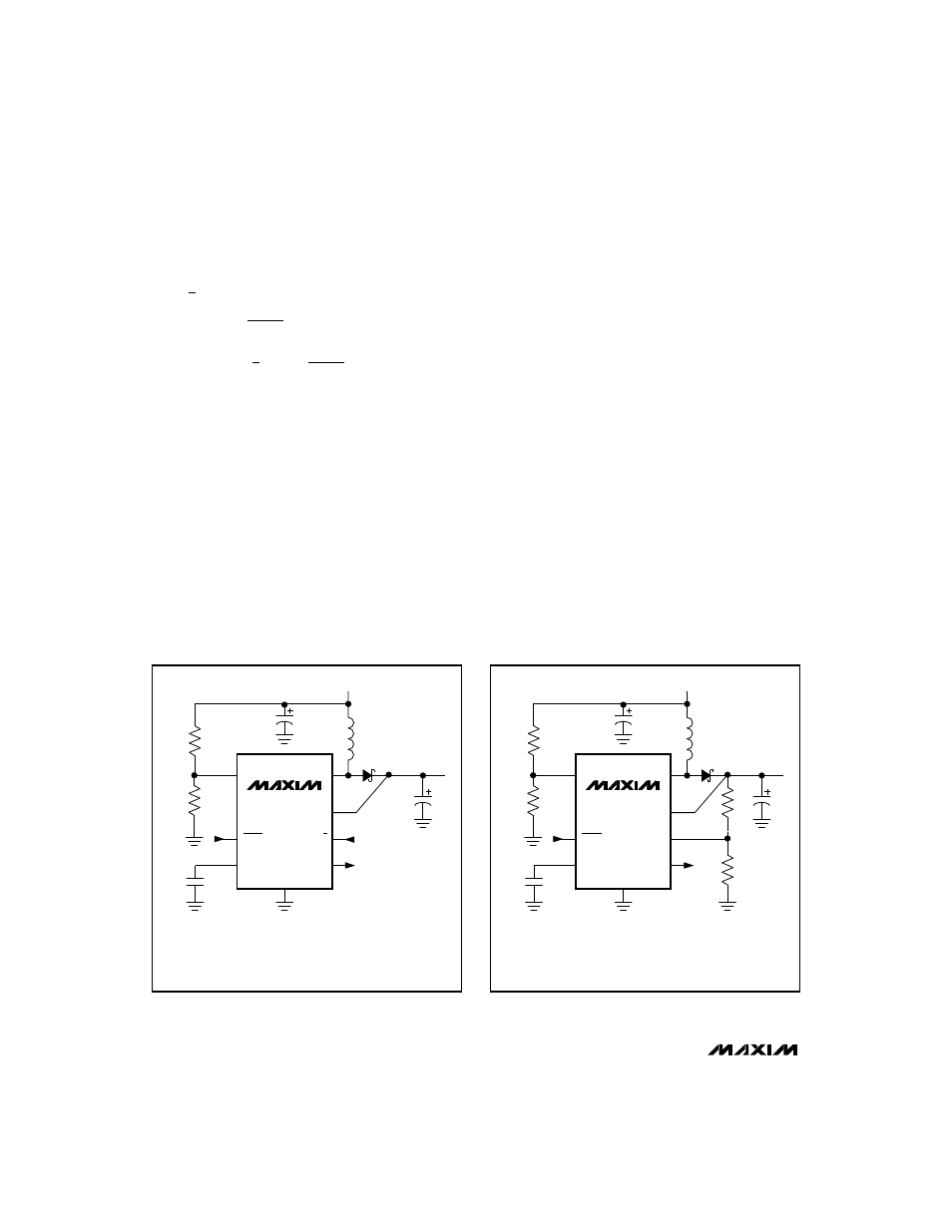
The MAX857/MAX859’s output voltage is set by two
resistors, R1 and R2 (Figure 2b), which form a voltage
divider between the output and FB. Use the following
equation to determine the output voltage:
R1 + R2
V
OUT
= V
REF
( _________ )
R2
where V
REF
= 1.25V.
To simplify resistor selection:
V
OUT
R1 = R2 ( _______ - 1)
V
REF
Since the input bias current at FB has a maximum value
of 100nA, large values (10k
Ω
to 300k
Ω
) can be used
for R1 and R2 with no significant accuracy loss. For 1%
error, the current through R1 should be at least 100
times FB’s bias current.
C1*
L1
V
IN
D1
1N5817
C2*
R1
R2
LX
OUT
FB
LBO
LBI
REF
SHDN
GND
R3
R4
C3
0.1
µ
F
V
OUT
5
1
3
8
6
2
4
7
MAX857/MAX859
*C1 = C2 = 68
µ
F FOR MAX857
47
µ
H
C1 = C2 = 22
µ
F FOR MAX859
C1*
L1
V
IN
D1
1N5817
C2*
R1
LX
OUT
3/5
LBO
LBI
REF
SHDN
GND
R3
R4
C3
0.1
µ
F
V
OUT
5
1
3
8
6
2
4
7
MAX856/MAX858
*C1 = C2 = 68
µ
F FOR MAX856
OUTPUT
SELECT
47
µ
H
C1 = C2 = 22
µ
F FOR MAX858
Figure 2b. Standard Application Circuit—Adjustable Output
Voltage
Figure 2a. Standard Application Circuit—Preset Output
Voltage
