Design procedure, Shdn – Rainbow Electronics MAX1606 User Manual
Page 8
MAX1606
28V Internal Switch LCD Bias Supply
with True Shutdown
8
_______________________________________________________________________________________
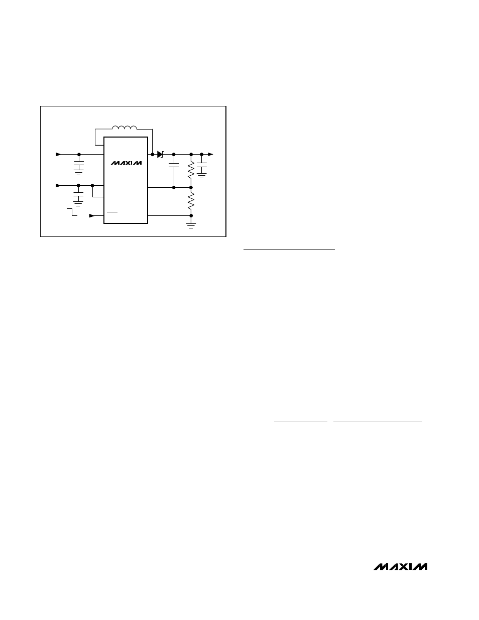
Setting the Output Voltage (FB)
Adjust the output voltage by connecting a voltage-
divider from the output (V
OUT
) to FB (Figure 3). Select
R2 between 10k
Ω and 200kΩ. Calculate R1 with the fol-
lowing equation:
R1 = R2 [(V
OUT
/ V
FB
) – 1]
where V
FB
= 1.25V and V
OUT
may range from V
BATT
to
28V. The input bias current of FB has a maximum value
of 100nA, which allows large-value resistors to be used.
For less than 1% error, the current through R2 should
be greater than 100 times the feedback input bias cur-
rent (I
FB
).
Current-Limit Select Pin (LIM)
The MAX1606 allows a selectable inductor current limit
of 125mA, 250mA, or 500mA (Figure 2). This allows
flexibility in designing for higher current applications or
for smaller, compact designs. The lower current limit
allows the use of a physically smaller inductor in space-
sensitive, low-power applications. Connect LIM to V
CC
for 500mA, leave floating for 250mA, or connect to
GND for 125mA.
Shutdown (
SHDN
)
Pull SHDN low to enter shutdown. During shutdown the
supply current drops to 0.1µA, the output is discon-
nected from the input, and LX enters a high-impedance
state. The capacitance and load at the output deter-
mine the rate at which V
OUT
decays. SHDN can be
pulled as high as 6V, regardless of the input and output
voltages.
With the typical step-up converter circuit, the output
remains connected to the input through the inductor and
output rectifier, holding the output voltage to one diode
drop below V
IN
when the converter is shutdown and
allowing the output to draw power from the input. The
MAX1606 features true shutdown, which uses an internal
P-channel MOSFET to disconnect the output from the
input when the MAX1606 is shutdown. This eliminates
power drawn from the input during shutdown.
Separate/Same Power for V
BATT
and V
CC
Separate voltage sources can supply the inductor
(V
BATT
) and the IC (V
CC
). Since the chip bias is provid-
ed by a logic supply (2.4V to 5.5V), this allows the out-
put power to be sourced directly from low-voltage
batteries (0.8V to 5.5V). Conversely, V
BATT
and V
CC
can also be supplied from one supply if it remains with-
in V
CC
’s operating limits (2.4V to 5.5V).
Design Procedure
Inductor Selection
Smaller inductance values typically offer smaller physi-
cal size for a given series resistance or saturation cur-
rent. Circuits using larger inductance values may start
up at lower input voltages and exhibit less ripple, but
also provide reduced output power. This occurs when
the inductance is sufficiently large to prevent the maxi-
mum current limit from being reached before the maxi-
mum on-time expires. The inductor’s saturation current
rating should be greater than the peak switching cur-
rent. However, it is generally acceptable to bias the
inductor into saturation by as much as 20%, although
this will slightly reduce efficiency.
Picking the Current Limit
The peak LX current limit (I
LX(MAX)
) required for the
application may be calculated from the following equa-
tion:
where t
OFF(MIN)
= 0.8µs, and V
BATT(MIN)
is the mini-
mum voltage used to supply the inductor. The set cur-
rent limit must be greater than this calculated value.
Select the appropriate current limit by connecting LIM
to V
CC
, GND, or leaving it unconnected (see Current-
Limit Select Pin and Figure 2).
Diode Selection
The high switching frequency of 500kHz requires a high-
speed rectifier. Schottky diodes, such as the Motorola
MBRS0530 or the Nihon EP05Q03L, are recommended.
To maintain high efficiency, the average current rating of
the Schottky diode should be greater than the peak
I
V
I
V
V
V
t
L
LX MAX
OUT
OUT MAX
BATT MIN
OUT
BATT MIN
OFF MIN
(
)
(
)
(
)
(
)
(
)
≥
Ч
+
−
(
)
Ч
Ч
2
V
BATT
= 0.8V TO 5.5V
V
CC
= 2.4V TO 5.5V
V
OUT
= 18V
ON
OFF
SHDN
V
CC
LIM
SW
BATT
GND
LX
FB
MAX1606
C
OUT
1
µF
C2
10
µF
C1
1
µF
C
FF
10pF
D1
R1
1M
Ω
R2
75k
L1
10
µH
Figure 3. Typical Application Circuit