Chip information, Table 2. component list for circuit of figure 2 – Rainbow Electronics MAX8724 User Manual
Page 26
MAX1908/MAX8724
Low-Cost Multichemistry Battery Chargers
26
______________________________________________________________________________________
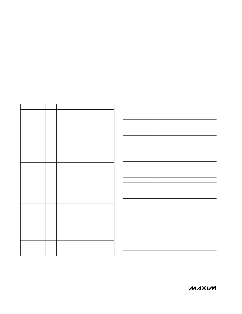
Table 2. Component List for Circuit of Figure 2
DESIGNATION
QTY
DESCRIPTION
C1
2
10µF, 50V 2220-size ceramic
capacitors
TDK C5750X7R1H106M
C4
1
22µF, 25V 2220-size ceramic
capacitor
TDK C5750X7R1E226M
C5
1
1µF, 25V X7R ceramic capacitor
(1206)
Murata GRM31MR71E105K
Taiyo Yuden TMK316BJ105KL
TDK C3216X7R1E105K
C9, C10
2
0.01µF, 16V cer am i c cap aci tor s ( 0402)
Murata GRP155R71E103K
Taiyo Yuden EMK105BJ103KV
TDK C1005X7R1E103K
C11, C14,
C15, C20
4
0.1µF, 25V X7R ceramic capacitors
(0603)
Murata GRM188R71E104K
TDK C1608X7R1E104K
C12, C13, C16
3
1µF, 6.3V X5R ceramic capacitors
(0603)
Murata GRM188R60J105K
Taiyo Yuden JMK107BJ105KA
TDK C1608X5R1A105K
D1 (optional)
1
10A Schottky diode (D-PAK)
Diodes, Inc. MBRD1035CTL
ON Semiconductor MBRD1035CTL
D2
1
Schottky diode
Central Semiconductor
CMPSH1–4
DESIGNATION
QTY
DESCRIPTION
D3
1
Schottky diode
Central Semiconductor CMPSH1-4
L1
1
10µH, 4.4A inductor
Sumida CDRH104R-100NC
TOKO 919AS-100M
N1
1
Dual, N-channel, 8-pin SO MOSFET
Fairchild FDS6990A or FDS6990S
P1
1
Single, P-channel, 8-pin SO MOSFET
Fairchild FDS6675
R5
1
1k
Ω
±5% resistor (0603)
R6
1
59k
Ω
±1% resistor (0603)
R7
1
19.6k
Ω
±1% resistor (0603)
R11
1
12k
Ω
±5% resistor (0603)
R12
1
15k
Ω
±5% resistor (0603)
R13
1
33
Ω
±5% resistor (0603)
R14
1
10.5k
Ω
±1% resistor (0603)
R15, R16
2
8.25k
Ω
±1% resistors (0603)
R17
1
19.1k
Ω
±1% resistor (0603)
R18
1
22k
Ω
±1% resistor (0603)
R19, R20
2
10k
Ω
±1% resistors (0603)
RS1
1
0.01
Ω
±1%, 0.5W 2010 sense resistor
Vishay Dale WSL2010 0.010 1.0%
IRC LRC-LR2010-01-R010-F
RS2
1
0.015
Ω
±1%, 0.5W 2010 sense
resistor
Vishay Dale WSL2010 0.015 1.0%
IRC LRC-LR2010-01-R015-F
U1
1
MAX1908ETI or MAX8724ETI
Chip Information
TRANSISTOR COUNT: 3772
PROCESS: BiCMOS
2) Place the IC and signal components. Keep the
main switching node (LX node) away from sensitive
analog components (current-sense traces and REF
capacitor).
Important: The IC must be no further
than 10mm from the current-sense resistors.
Keep the gate-drive traces (DHI, DLO, and BST)
shorter than 20mm, and route them away from the
current-sense lines and REF. Place ceramic
bypass capacitors close to the IC. The bulk capac-
itors can be placed further away.
3) Use a single-point star ground placed directly
below the part at the backside exposed pad of the
MAX1908/MAX8724. Connect the power ground
and normal ground to this node.