Applications information, Power-down modes, Internal clock – Rainbow Electronics MAX1189 User Manual
Page 8: Starting a conversion, Selecting standby or shutdown mode
MAX1179/MAX1187/MAX1189
Track and Hold (T/H)
In track mode, the internal hold capacitor acquires the
analog signal (see Figure 4). In hold mode, the T/H
switches open and the capacitive DAC samples the
analog input. During the acquisition, the analog input
(AIN) charges capacitor C
HOLD
. The acquisition ends
on the second falling edge of CS. At this instant, the
T/H switches open. The retained charge on C
HOLD
rep-
resents a sample of the input. In hold mode, the capac-
itive DAC adjusts during the remainder of the
conversion time to restore node T/H OUT to zero within
the limits of a 16-bit resolution. Force CS low to put
valid data on the bus after conversion is complete.
Power-Down Modes
Select standby mode or shutdown mode with R/C during
the second falling edge of CS (see Selecting Standby or
Shutdown Mode section). The MAX1179/MAX1187/
MAX1189 automatically enter either standby mode (ref-
erence and buffer on) or shutdown (reference and buffer
off) after each conversion depending on the status of
R/C during the second falling edge of CS.
Internal Clock
The MAX1179/MAX1187/MAX1189 generate an internal
conversion clock to free the microprocessor from the bur-
den of running the SAR conversion clock. Total conver-
sion time after entering hold mode (second falling edge of
CS) to end-of-conversion (EOC) falling is 4.7µs (max).
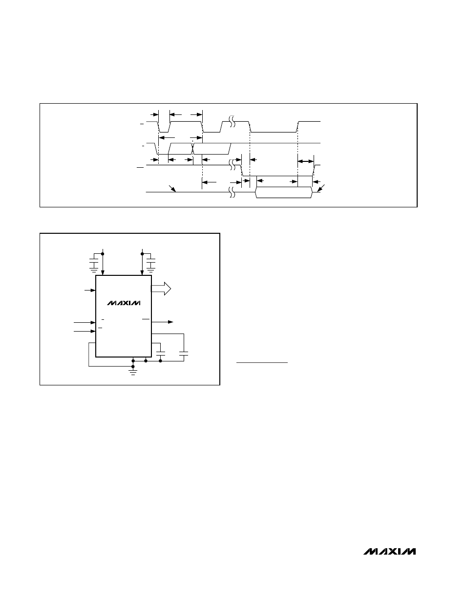
Applications Information
Starting a Conversion
CS and R/C control acquisition and conversion in the
MAX1179/MAX1187/MAX1189 (see Figure 2). The first
falling edge of CS powers up the device and puts it in
acquire mode if R/C is low. The convert start (CS) is
ignored if R/C is high. The MAX1179/MAX1187/
MAX1189 need at least 12ms (C
REFADJ
= 0.1µF, C
REF
= 10µF) for the internal reference to wake up and settle
before starting the conversion, if powering up from
shutdown. Reset the MAX1179/MAX1187/ MAX1189 by
toggling RESET with CS high. The next falling edge of
CS begins acquisition.
Selecting Standby or Shutdown Mode
The MAX1179/MAX1187/MAX1189 have a selectable
standby or low-power shutdown mode. In standby
mode, the ADC’s internal reference and reference
buffer do not power down between conversions, elimi-
nating the need to wait for the reference to power up
before performing the next conversion. Shutdown mode
powers down the reference and reference buffer after
16-Bit, 135ksps, Single-Supply ADCs with
Bipolar Analog Input Range
8
_______________________________________________________________________________________
Figure 2. MAX1179/MAX1187/MAX1189 Timing Diagram
t
CSL
t
CSH
t
ACQ
t
DH
R/C
CS
EOC
D0–D15
t
DS
t
DV
t
EOC
t
DO
t
BR
t
CONV
HIGH-Z
REF POWER-
DOWN CONTROL
HIGH-Z
DATA VALID
Figure 3. Typical Application Circuit for the MAX1179/MAX1187/
MAX1189
MAX1179
MAX1187
MAX1189
ANALOG
INPUT
AIN
AV
DD
+5V ANALOG
+5V DIGITAL
DV
DD
D0–D15
16-BIT
WIDE
µP DATA
BUS
10
µF
0.1
µF
0.1
µF
0.1
µF
R/C
CS
AGND DGND
REFADJ
REF
EOC
RESET