Typical operating characteristics, Electrical characteristics (continued) – Rainbow Electronics MAX1420 User Manual
Page 5
MAX1420
12-Bit, 60Msps, +3.3V, Low-Power ADC
with Internal Reference
_______________________________________________________________________________________
5
Note 1: Internal reference, REFIN bypassed to AGND with a combination of 0.22µF in parallel with 1nF capacitor.
Note 2: External +2.048V reference applied to REFIN.
Note 3: Internal reference disabled. V
REFIN
= 0, V
REFP
= +2.162V, V
CML
= +1.65V, and V
REFN
= +1.138V.
Note 4: IMD is measured with respect to either of the fundamental tones.
Note 5: Specifies the common-mode range of the differential input signal supplied to the MAX1420.
Note 6: V
DIFF
= V
REFP
- V
REFN
.
Note 7: Input bandwidth is measured at a 3dB level.
Note 8: V
REFIN
is internally biased to +2.048V through a 10k
Ω resistor.
Note 9: Measured as the ratio of the change in mid-scale offset voltage for a ±5% change in V
AVDD
, using the internal reference.
ELECTRICAL CHARACTERISTICS (continued)
(V
AVDD
= V
DVDD
= +3.3V, AGND = DGND = 0, V
IN
= ±1.024V, differential input voltage at -0.5dB FS, internal reference, f
CLK
=
62.5MHz (50% duty cycle), digital output load C
L
≈ 10pF, T
A
= T
MIN
to T
MAX
, unless otherwise noted. Typical values are at
T
A
= +25
°C.)
PARAMETER
SYMBOL
CONDITIONS
MIN
TYP
MAX
UNITS
Power Dissipation In Shutdown
P
DISS
PD = V
DVDD
10
µW
Power-Supply Rejection Ratio
PSRR
(Note 9)
±1
mV/V
TIMING CHARACTERISTICS
Maximum Clock Frequency
f
CLK
60
MHz
Clock High
t
CH
Figure 6, clock period 16.667ns
8.33
ns
Clock Low
t
CL
Figure 6, clock period 16.667ns
8.33
ns
Pipeline Delay (Latency)
Figure 6
7
f
CLK
cycles
Aperture Delay
t
AD
Figure 10
2
ns
Aperture Jitter
t
AJ
Figure 10
2
ps
Data Output Delay
t
OD
Figure 6
5
10
14
ns
Bus Enable Time
t
BE
Figure 5
5
ns
Bus Disable Time
t
BD
Figure 5
5
ns
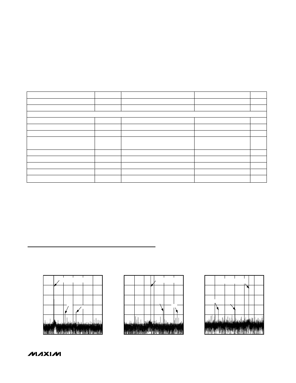
Typical Operating Characteristics
(V
AVDD
= V
DVDD
= +3.3V, AGND = DGND = 0, V
IN
= ±1.024V, differential input voltage at -0.5dB FS, f
CLK
= 60.006MHz (50% duty
cycle), digital output load C
L
= 10pF, T
A
= T
MIN
to T
MAX
, unless otherwise noted. Typical values are at T
A
= +25
°C.)
-120
-80
-100
-40
-60
-20
0
0
30
FFT PLOT (8192-POINT DATA RECORD)
DIFFERENTIAL INPUT
MAX1420 toc01
ANALOG INPUT FREQUENCY (MHz)
AMPLITUDE (dB)
10
15
5
20
25
HD2
HD3
f
IN
= 5.5449583MHz
-120
-80
-100
-40
-60
-20
0
0
30
FFT PLOT (8192-POINT DATA RECORD)
DIFFERENTIAL INPUT
MAX1420 toc02
ANALOG INPUT FREQUENCY (MHz)
AMPLITUDE (dB)
10
15
5
20
25
HD2
HD3
f
IN
= 13.4119138MHz
-120
-80
-100
-40
-60
-20
0
0
30
FFT PLOT (8192-POINT DATA RECORD)
DIFFERENTIAL INPUT
MAX1420 toc03
ANALOG INPUT FREQUENCY (MHz)
AMPLITUDE (dB)
10
15
5
20
25
HD2
HD3
f
IN
= 37.701219MHz