Rainbow Electronics MAX1420 User Manual
Page 11
MAX1420
12-Bit, 60Msps, +3.3V, Low-Power ADC
with Internal Reference
______________________________________________________________________________________
11
cations that require increased accuracy and a different
input voltage range.
The MAX1420 provides three modes of reference oper-
ation:
• Internal reference mode
• Buffered external reference mode
• Unbuffered external reference mode
In internal reference mode, the on-chip +2.048V
bandgap reference is active and REFIN, REFP, CML,
and REFN are left floating. For stability purposes,
bypass REFIN, REFP, REFN and CML with a capacitor
network of 0.22µF in parallel with a 1nF capacitor to
AGND.
In buffered external reference mode, the reference volt-
age levels can be adjusted externally by applying a
stable and accurate voltage at REFIN.
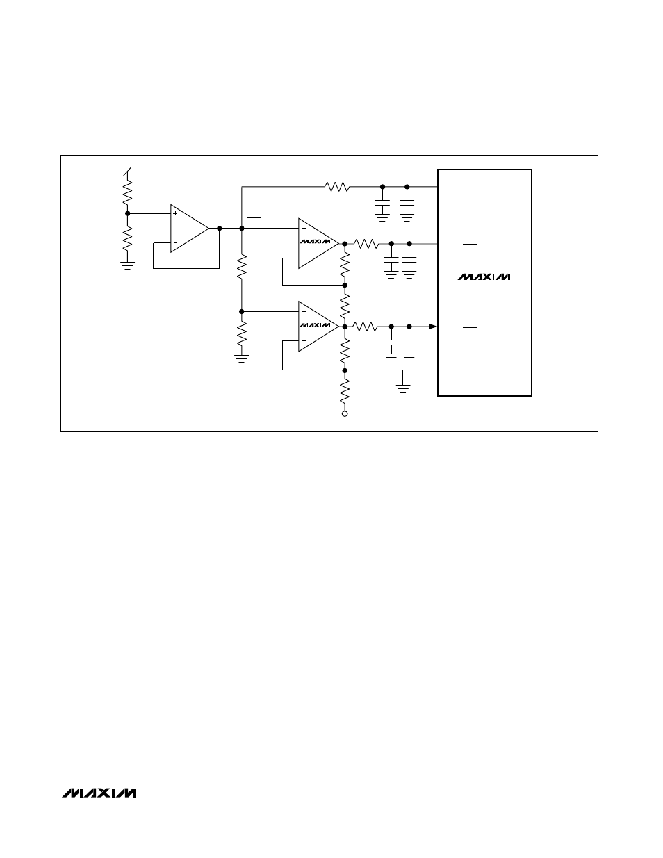
In unbuffered external reference mode, REFIN is con-
nected to AGND, thereby deactivating the on-chip
buffers of REFP, CML, and REFN. With their buffers
shut down, these nodes become high impedance and
can be driven by external reference sources, as shown
in Figure 3.
Clock Inputs (CLK,
CLK
)
The MAX1420’s CLK and CLK inputs accept both dif-
ferential and single-ended input operation and accept
CMOS-compatible clock signals. If CLK is driven with a
single-ended clock signal, bypass CLK with a 0.1µF
capacitor to AGND. Since the interstage conversion of
the device depends on the repeatability of the rising
and falling edges of the external clock, use a clock with
low jitter and fast rise and fall times (< 2ns). Sampling
occurs on the rising edge of the clock signal, requiring
this edge to have the lowest possible jitter. Any signifi-
cant aperture jitter would limit the SNR performance of
the ADC according to the following relationship:
where f
IN
represents the analog input frequency and
t
AJ
is the aperture jitter. Clock jitter is especially critical
for high input frequency applications. The clock input
should always be considered as an analog signal and
routed away from any analog or digital signal lines.
The MAX1420 clock input operates with a voltage
threshold set to AV
DD
/2. Clock inputs must meet the
specifications for high and low periods as stated in the
Electrical Characteristics.
SNR
f
t
dB
IN
AJ
=
Ч
Ч
Ч
20
1
2
10
log
π
MAX1420
REFIN
REFN
R
50
Ω
R
R
R
R
0.5V
R
50
Ω
50
Ω
R
R
AV
DD
CML
1nF
0.22
µF
1nF
0.22
µF
1nF
0.22
µF
AGND
AV
DD
2
AV
DD
4
MAX4284
MAX4284
( )
REFP
0.5V
( )
AV
DD
2
0.5V
( )
AV
DD-
2
AV
DD
2
AV
DD
4
AV
DD
2
Figure 3. Unbuffered External Reference Drive—Internal Reference Disabled