Internal clock – Rainbow Electronics MAX1109 User Manual
Page 14
MAX1108/MAX1109
Single-Supply, Low-Power,
2-Channel, Serial 8-Bit ADCs
14
______________________________________________________________________________________
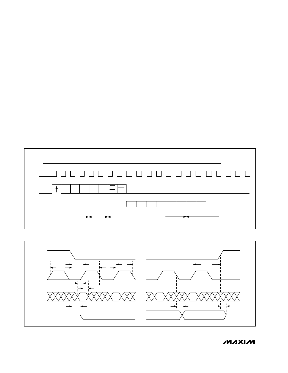
initiated. The MSB successive-approximation bit deci-
sion is made on the rising edge of the seventh SCLK.
On the falling edge of the eighth SCLK, the MSB is
clocked out on the DOUT pin; on each of the next
seven SCLK falling edges, the remaining bits of conver-
sion are clocked out. Zeros are clocked out on DOUT
after the LSB has been clocked out, until CS is dis-
abled. Then DOUT becomes high impedance and the
part is ready for another conversion (Figure 6).
The conversion must complete in 1ms, or droop on the
sample-and-hold capacitors may degrade conversion
results. Use internal clock mode if the serial-clock fre-
quency is less than 50kHz, or if serial-clock interrup-
tions could cause the conversion interval to exceed
1ms.
Internal Clock
Internal clock mode frees the µP from the burden of
running the SAR conversion clock. This allows the con-
version results to be read back at the processor’s con-
venience, at any clock rate up to 2MHz.
An internal register stores data when the conversion is
in progress. On the falling edge of the fourth SCLK,
track mode is enabled, and on the falling edge of the
eighth SCLK, acquisition is complete and internal con-
version is initiated. The internal 400kHz clock com-
pletes the conversion in 20µs typically (35µs max), at
which time the MSB of the conversion is present at the
DOUT pin. The falling edge of SCLK clocks the remain-
ing data out of this register at any time after the conver-
sion is complete (Figure 8).
CS
SCLK
DIN
DOUT
1
4
8
12
16
20
START
SEL2
MSB
LSB
SEL1
SEL0
I/ECLK I/EREF
REF
SHDN
SHDN
D7
MSB
LSB
D6
D5
D4
D3
D2
D1
D0
IDLE
IDLE
t
CONV
t
ACQ
A/D STATE
Figure 6. Single Conversion Timing, External Clock Mode
• • •
• • •
• • •
• • •
CS
SCLK
DIN
DOUT
t
CSH
t
CSS
t
CL
t
DS
t
DH
t
DV
t
CH
t
DO
t
TR
t
CSH
Figure 7. Detailed Serial-Interface Timing