Detailed description, Analog inputs track/hold, Modes of operation – Rainbow Electronics MAX1109 User Manual
Page 10
MAX1108/MAX1109
Single-Supply, Low-Power,
2-Channel, Serial 8-Bit ADCs
10
______________________________________________________________________________________
_______________Detailed Description
The MAX1108/MAX1109 analog-to-digital converters
(ADCs) use a successive-approximation conversion
technique and input track/hold (T/H) circuitry to convert
an analog signal to an 8-bit digital output. A flexible
serial interface provides easy interface to microproces-
sors (µPs). No external hold capacitors are required. All
of the MAX1108/MAX1109 operating modes are soft-
ware-configurable: internal or external reference, inter-
nal or external conversion clock, single-ended unipolar
or pseudo-differential unipolar/bipolar conversion, and
power down (Table 1).
Analog Inputs
Track/Hold
The input architecture of the ADCs is illustrated in the
equivalent-input circuit of Figure 4 and is composed of
the T/H, the input multiplexer, the input comparator, the
switched capacitor DAC, the reference, and the auto-
zero rail.
The analog-inputs configuration is determined by the
control-byte through the serial interface as shown in
Table 2 (see
Modes of Operation
section and Table 1).
The eight modes of operation include single-ended,
pseudo-differential, unipolar/bipolar, and a V
DD
moni-
toring mode. During acquisition and conversion, only
one of the switches in Figure 4 is closed at any time.
The T/H enters its tracking mode on the falling clock
edge after bit 4 (SEL0) of the control byte has been
shifted in. It enters its hold mode on the falling edge
after the bit 2 (I/EREF) of the control byte has been
shifted in.
For example, If CH0 and COM are chosen (SEL2 =
SEL1 = SEL0 = 1) for conversion, CH0 is defined as the
sampled input (SI), and COM is defined as the refer-
ence input (RI). During acquisition mode, the CH0
switch and the T/H switch are closed, charging the
V
DD
3k
C
LOAD
DGND
DOUT
C
LOAD
DGND
3k
DOUT
a) High-Z to V
OH
and V
OL
to V
OH
b) High-Z to V
OL
and V
OH
to V
OL
Figure 1. Load Circuits for Enable Time
V
DD
3k
C
LOAD
DGND
DOUT
C
LOAD
DGND
3k
DOUT
a) V
OH
to High-Z
b) V
OL
to High-Z
Figure 2. Load Circuits for Disable Time
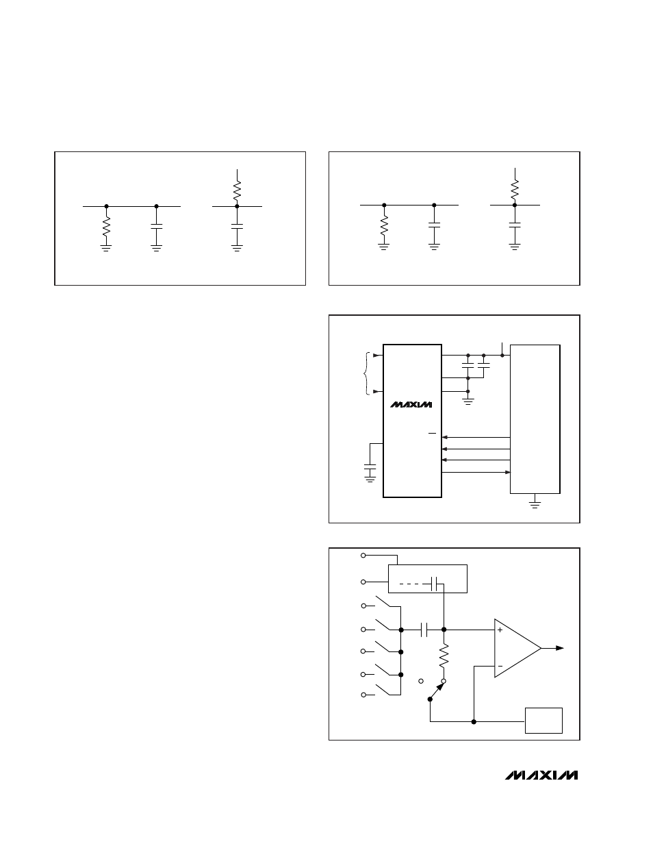
V
DD
I/O
SCK (SK)
MOSI (SO)
MISO (SI)
V
SS
DOUT
DIN
SCLK
CS
COM
GND
V
DD
CH1
1
µ
F
0.1
µ
F
1
µ
F
CH0
ANALOG
INPUTS
MAX1108
MAX1109
CPU
V
DD
REF
Figure 3. Typical Operating Circuit
CH0
COM
V
DD
/ 2
GND
CH1
REF
GND
C
HOLD
CAPACITIVE DAC
COMPARATOR
18pF
R
IN
6.5k
AUTOZERO
RAIL
TRACK
HOLD
Figure 4. Equivalent Input Circuit