Note 2), Note 4), Note 6) – Rainbow Electronics LM88 User Manual
Page 4: Note 5), Note 7), Note 8), Note 9), Note 10), Lm88 electrical characteristics, Lm88
LM88 Electrical Characteristics
(Continued)
Note 2: When the input voltage (V
I
) at any pin exceeds the power supply (V
I
<
GND or V
I
>
V
+
), the current at that pin should be limited to 5mA. The 20mA
maximum package input current rating limits the number of pins that can safely exceed the power supplies with an input current of 5mA to four.
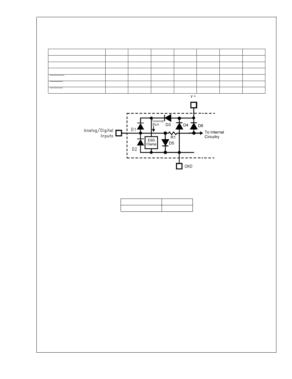
Note 3: Parasitics or ESD protection circuitry are shown in the diagram found below. The ESD Clamp circtuitry is triggered on when there is an ESD event. The table
maps what devices appear on the different pins.
Pin Name
D1
D2
D3
D4
D5
D6
R1
D0+
X
X
X
X
X
50
Ω
D−
X
X
X
X
X
X
50
Ω
D1+
X
X
X
X
X
50
Ω
O_CRIT
X
X
X
X
0
Ω
O_SP1
X
X
X
X
0
Ω
O_SP0
X
X
X
X
0
Ω
10132604
Note 4: The maximum power dissipation must be derated at elevated temperatures and is dictated by T
Jmax
(maximum junction temperature),
θ
JA
(junction to
ambient thermal resistance) and T
A
(ambient temperature). The maximum allowable power dissipation at any temperature is P
D
= (T
Jmax
–T
A
)/
θ
JA
or the number
given in the Absolute Maximum Ratings, whichever is lower. For this device, T
Jmax
= 125˚C. For this device the typical thermal resistance (
θ
JA
) of the different
package types when board mounted follow:
Package Type
θ
JA
MUA08A
250˚C/W
Note 5: The human body model is a 100pF capacitor discharged through a 1.5k
Ω
resistor into each pin. The machine model is a 200pF capacitor discharged directly
into each pin.
Note 6: See the URL ”http://www.national.com/packaging/“ for other recomdations and methods of soldering surface mount devices.
Note 7: Typicals are at T
J
= T
A
= 25˚C and represent most likely parametric norm.
Note 8: Limits are guaranteed to National’s AOQL (Average Outgoing Quality Level).
Note 9: These are sample temperature ranges, contact the factory for other temperature ranges. Performance is dependent on temperature range.
Note 10: The two I
OH
specifications are intended to describe two operating regions of the output voltage. In Region 1, V
+
− 0.6V and below, there is normal leakage
current, 2µA (max). In Region 2, V
+
− 0.6V to V
+
, there is additional current flowing caused by the ESD protection circuitry (see Figure in Note 3). The maximum
current flow is under short circuit conditions as specified at 40µA (max). Under normal operating conditions a pull-resistor (R) will be used. The voltage drop across
this pull-up resistor caused by the 2µA normal leakage current with large values of R (much greater than 100k) will bias diode D1 into the cutoff region causing the
additional current to be negligible in the voltage drop calculation. With low values of R more current will flow as in the case of a 1.1k pull-up, 20µA may flow causing
less than 22mV of voltage drop.
LM88
www.national.com
4