Applications information, Dynamic performance, Table 2. bypassing – Rainbow Electronics MAX1003 User Manual
Page 10
MAX1003
Low-Power, 90Msps, Dual 6-Bit ADC
10
______________________________________________________________________________________
__________Applications Information
The MAX1003 is designed with separate analog and
digital power-supply and ground connections to isolate
high-current digital noise spikes from the more sensi-
tive analog circuitry. The high-current digital output
ground (OGND) and analog ground (GND) should be
at the same DC level, connected at only one location
on the board. This will provide best noise immunity and
improved conversion accuracy. Use of separate
ground planes is strongly recommended.
The entire board needs good DC bypassing for both
analog and digital supplies. Place the power-supply
bypass capacitors close to where the power is routed
onto the board, i.e., close to the connector. 10µF elec-
trolytic capacitors with low-ESR ratings are recom-
mended. For best effective bits performance, minimize
capacitive loading at the digital outputs. Keep the digi-
tal output traces as short as possible.
The MAX1003 requires a +5V ±5% power supply for
the analog supply (V
CC
) and a +3.3V ±300mV power
supply connected to V
CCO
for the logic outputs.
Bypass each of the V
CC_
supply pins to its respective
GND with high-quality ceramic capacitors located as
close to the package as possible (Table 2). Consult the
evaluation kit manual for a suggested layout and
bypassing scheme.
_____________Dynamic Performance
Signal-to-noise and distortion (SINAD) is the ratio of the
fundamental input frequency’s RMS amplitude to all
other ADC output signals. The output spectrum is limit-
ed to frequencies above DC and below one-half the
ADC sample rate.
The theoretical minimum analog-to-digital noise is
caused by quantization error, and results directly from
the ADC’s resolution: SNR = (6.02N + 1.76)dB, where
N is the number of bits of resolution. Therefore, a per-
fect 6-bit ADC can do no better than 38dB.
The FFT Plot (see
Typical Operating Characteristics
)
shows the result of sampling a pure 20MHz sinusoid at
a 90MHz clock rate. This FFT plot of the output shows
the output level in various spectral bands. The plot has
been averaged to reduce the quantization noise floor
and reveal the low-amplitude spurs. This emphasizes
the excellent spurious-free dynamic range of the
MAX1003.
The effective resolution (or effective number of bits) the
ADC provides can be measured by transposing the
equation that converts resolution to SINAD: N =
(SINAD - 1.76) / 6.02 (see
Typical Operating
Characteristics
).
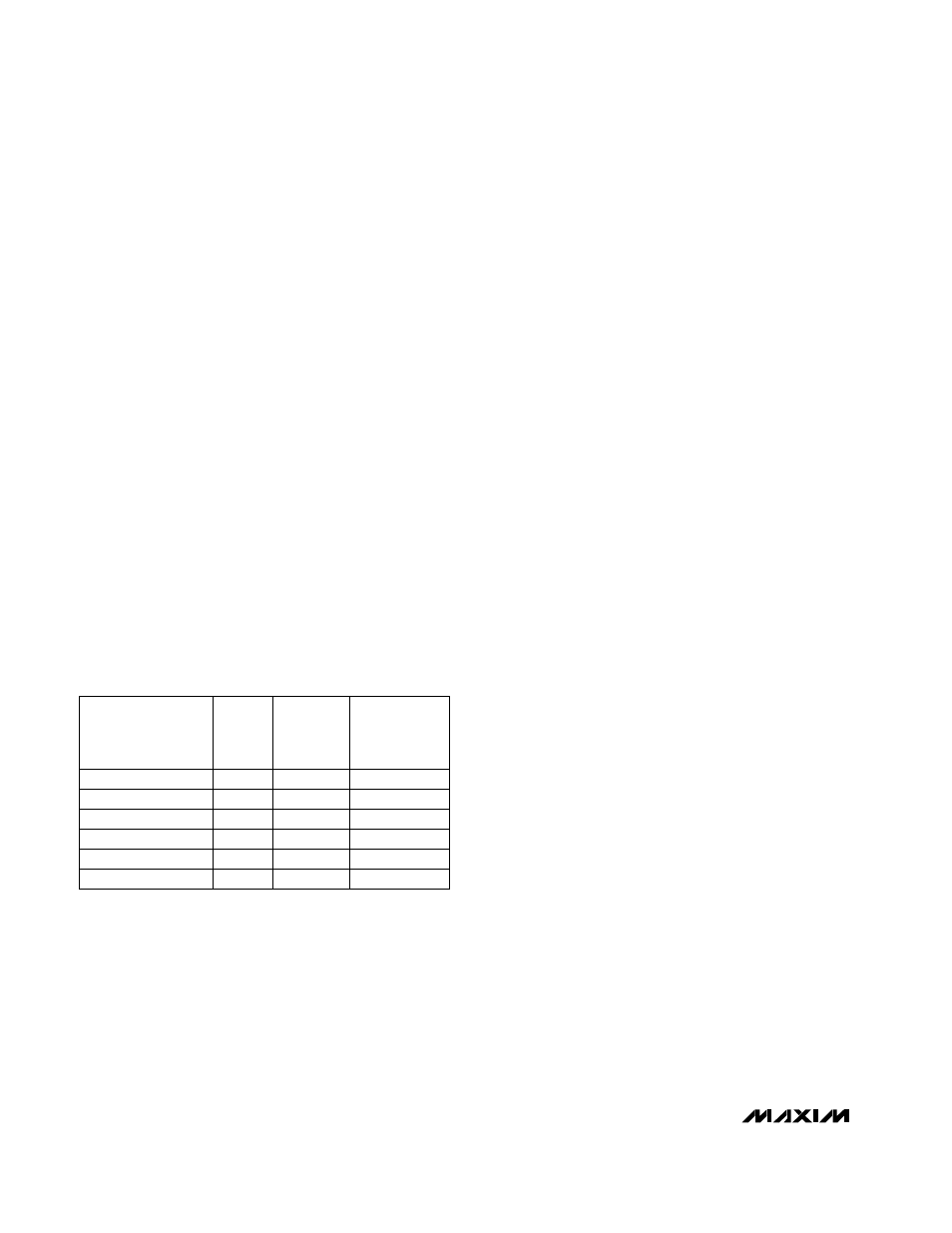
Table 2. Bypassing
0.01µF
Oscillator/Clock
0.01µF
Converter
SUPPLY
FUNCTION
0.01µF
Analog Inputs
CAPACITOR
VALUE
47pF
Digital I-Output
0.01µF
Buffer
47pF
Digital Q-Output
27
19
11
27
12
BYPASS
TO
GND/
OGND
7
28
36
8
26
13
V
CC
/
V
CCO
6