Max1510 low-voltage ddr linear regulator – Rainbow Electronics MAX1510 User Manual
Page 2
MAX1510
Low-Voltage DDR Linear Regulator
2
_______________________________________________________________________________________
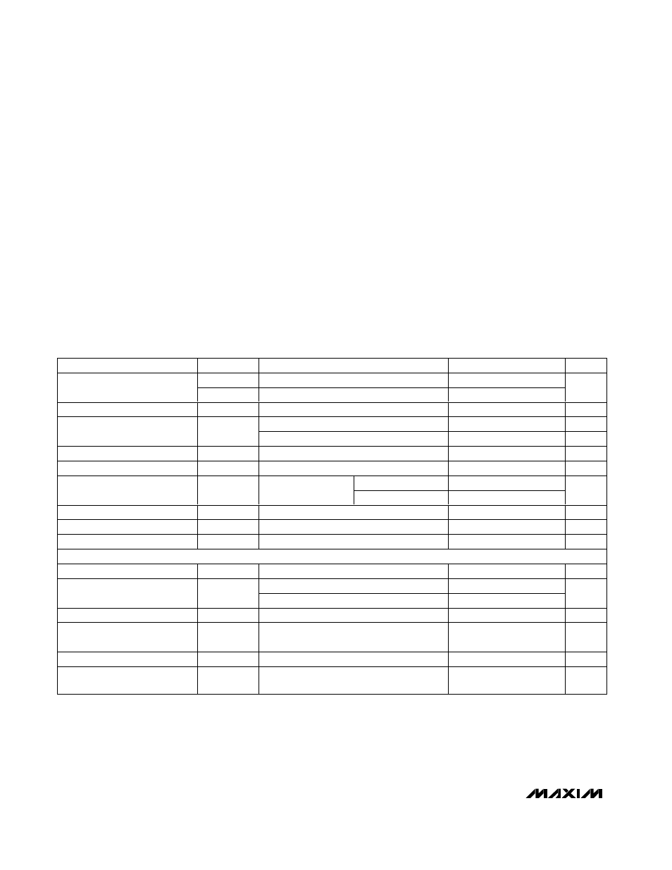
ABSOLUTE MAXIMUM RATINGS
ELECTRICAL CHARACTERISTICS
(V
IN
= 1.8V, V
CC
= 3.3V, V
REFIN
= V
OUTS
= 1.25V,
SHDN = V
CC
, circuit of Figure 1, T
A
= -40
°C to +85°C, unless otherwise noted.
Typical values are at T
A
= +25
°C.) (Note 1)
Stresses beyond those listed under “Absolute Maximum Ratings” may cause permanent damage to the device. These are stress ratings only, and functional
operation of the device at these or any other conditions beyond those indicated in the operational sections of the specifications is not implied. Exposure to
absolute maximum rating conditions for extended periods may affect device reliability.
IN to PGND...............................................................-0.3V to +4V
OUT to PGND ..............................................-0.3V to (V
IN
+ 0.3V)
OUTS to AGND ............................................-0.3V to (V
IN
+ 0.3V)
V
CC
to AGND............................................................-0.3V to +4V
REFIN, REFOUT,
SHDN, PGOOD to AGND ..-0.3V to (V
CC
+ 0.3V)
PGND to AGND .....................................................-0.3V to +0.3V
REFOUT Short Circuit to AGND .................................Continuous
OUT Continuous RMS Current: 100s ..................................
±1.6A
1s......................................±2.5A
Continuous Power Dissipation (T
A
= +70°C)
10-Pin 3mm x 3mm Thin DFN
(derated 24.4mW/
°C above +70°C)...........................1951mW
Operating Temperature Range
MAX1510ETB...................................................-40°C to +85°C
Junction Temperature ......................................................+150°C
Storage Temperature Range .............................-65°C to +150°C
Lead Temperature (soldering, 10s) .................................+300°C
PARAMETER
SYMBOL
CONDITIONS
MIN
TYP
MAX
UNITS
V
IN
Power input
1.1
3.6
Input Voltage Range
V
CC
Bias supply
2.7
3.6
V
Quiescent Supply Current (V
CC
)
I
CC
Load = 0, V
REFIN
> 0.45V
0.7
1.3
mA
SHDN = GND, V
REFIN
> 0.45V
350
600
µA
Shutdown Supply Current (V
CC
)
I
CC(SHDN)
SHDN = GND, REFIN = GND
50
100
µA
Quiescent Supply Current (V
IN
)
I
IN
Load = 0
0.4
10
mA
Shutdown Supply Current (V
IN
)
I
IN(SHDN)
SHDN = GND
0.1
10
µA
T
A
= 25°C
-4
0
+4
Feedback-Voltage Error
V
OUTS
REFIN to OUTS
I
OUT
=
±200mA
T
A
= -40°C to +85°C
-6
+6
mV
Load-Regulation Error
-1A
≤ I
OUT
≤ +1A
-15
+15
mV
Line-Regulation Error
1.4V
≤ V
IN
≤ 3.3V, I
OUT
= ±100mA
1
mV
OUTS Input Bias Current
I
OUTS
-1
+1
µA
OUTPUT
Output Adjust Range
0.5
1.5
V
High-side MOSFET (source) (I
OUT
= 0.1A)
0.10
0.25
OUT On-Resistance
Low-side MOSFET (sink) (I
OUT
= -0.1A)
0.10
0.25
Ω
Output Current Slew Rate
C
OUT
= 100µF, I
OUT
= 0.1A to 2A
3
A/µs
OUT Power-Supply Rejection
Ratio
PSRR
10Hz < f < 10kHz, I
OUT
= 200mA,
C
OUT
= 100µF
80
dB
OUT to OUTS Resistance
R
OUTS
12
k
Ω
Discharge MOSFET On-
Resistance
R
DISCHARGE
SHDN = GND
8
Ω