Max1510 low-voltage ddr linear regulator – Rainbow Electronics MAX1510 User Manual
Page 11
MAX1510
Low-Voltage DDR Linear Regulator
______________________________________________________________________________________
11
For a step voltage change at REFIN, the rate of change
of the output voltage is limited by the total output
capacitance, the current limit, and the load during the
transition. Adding a capacitor across REFIN and AGND
filters noise and controls the rate of change of the
REFIN voltage during dynamic transitions. With the
additional capacitance, the REFIN voltage slews
between the two set points with a time constant given
by R
EQ
x C
REFIN
, where R
EQ
is the equivalent parallel
resistance seen by the slew capacitor.
Operating Region and Power Dissipation
The maximum power dissipation of the MAX1510
depends on the thermal resistance of the 10-pin TDFN
package and the circuit board, the temperature differ-
ence between the die and ambient air, and the rate of
airflow. The power dissipated in the device is:
P
SRC
= I
SRC
x (V
IN
– V
OUT
)
P
SINK
= I
SINK
x V
OUT
The resulting maximum power dissipation is:
where T
J(MAX)
is the maximum junction temperature
(+150°C), T
A
is the ambient temperature,
θ
JC
is the
thermal resistance from the die junction to the package
case, and
θ
CA
is the thermal resistance from the case
through the PC board, copper traces, and other materi-
als to the surrounding air. For optimum power dissipa-
tion, use a large ground plane with good thermal
contact to the backside pad, and use wide input and
output traces.
When 1 square inch of copper is connected to the
device, the maximum allowable power dissipation of a
10-pin DFN package is 1951mW. The maximum power
dissipation is derated by 24.4mW/°C above T
A
= +70°C.
Extra copper on the PC board increases thermal mass
and reduces thermal resistance of the board. Refer to
the MAX1510 evaluation kit for a layout example.
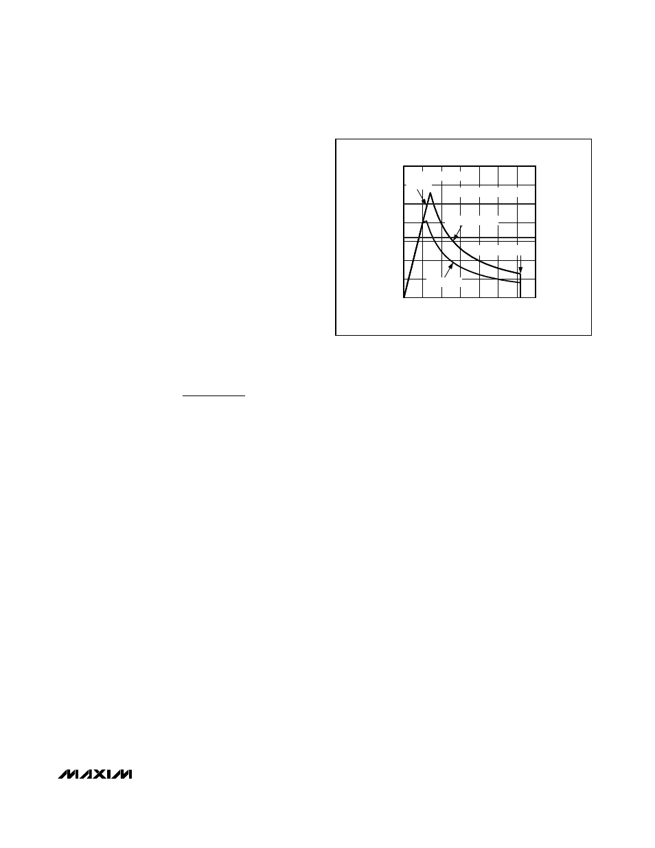
The MAX1510 delivers up to 3A and operates with input
voltages up to 3.6V, but not simultaneously. High output
currents can only be achieved when the input-output
differential voltages are low (Figure 5).
Dropout Operation
A regulator’s minimum input-to-output voltage differen-
tial (dropout voltage) determines the lowest usable sup-
ply voltage. Because the MAX1510 uses an n-channel
pass transistor, the dropout voltage is a function of the
drain-to-source on-resistance (R
DS(ON)
= 0.25
Ω max)
multiplied by the load current (see the Typical
Operating Characteristics):
V
DROPOUT
= R
DS(ON)
x I
OUT
For low output-voltage applications the sink current is
limited by the output voltage and the R
DS(ON)
of the
MOSFET.
Input Capacitor Selection
Bypass IN to PGND with a 10µF or greater ceramic
capacitor. Bypass V
CC
to AGND with a 1µF ceramic
capacitor for normal operation in most applications.
Typically, the LDO is powered from the output of a
step-down controller (memory supply) that has addi-
tional bulk capacitance (polymer or tantalum) and dis-
tributed ceramic capacitors.
Output Capacitor Selection
The MAX1510 output stability is independent of the out-
put capacitance for C
OUT
from 10µF to 220µF.
Capacitor ESR between 2m
Ω and 50mΩ is needed to
maintain stability. Within the recommended capaci-
tance and ESR limits, the output capacitor should be
chosen to provide good transient response.
∆I
OUT(P-P)
x ESR =
∆V
OUT(P-P)
where
∆I
OUT(P-P)
is the maximum peak-to-peak load-
current step (typically equal to the maximum source
load plus the maximum sink load), and
∆V
OUT(P-P)
is
the allowable peak-to-peak voltage tolerance.
Using larger output capacitance can improve efficiency
in applications where the source and sink currents
change rapidly. The capacitor acts as a reservoir for
the rapid source and sink currents, so no extra current
is supplied by the MAX1510 or discharged to ground,
improving efficiency.
P
T
T
DIS MAX
J MAX
A
JC
CA
(
)
(
)
=
+
-
θ
θ
0
1.0
0.5
2.0
1.5
3.0
2.5
3.5
0
1.0
1.5
0.5
2.0
2.5
3.0
3.5
SAFE OPERATING REGION
INPUT-OUTPUT DIFFERENTIAL VOLTAGE (V)
MAXIMUM OUTPUT CURRENT (A)
MAXIMUM CURRENT LIMIT
100s RMS
LIMIT
1s RMS
LIMIT
T
A
= +100°C
T
A
= 0°C TO +70°C
DROPOUT VOLTAGE
LIMITED
V
IN(MAX)
- V
OUT(MIN)
Figure 5. Power Operating Region—Maximum Output Current
vs. Input-Output Differential Voltage