Chip topography, Table 1. trouble-shooting chart – Rainbow Electronics MAX742 User Manual
Page 12
MAX742
Switch-Mode Regulator with
+5V to ±12V or ±15V Dual Output
12
______________________________________________________________________________________
Table 1. Trouble-Shooting Chart
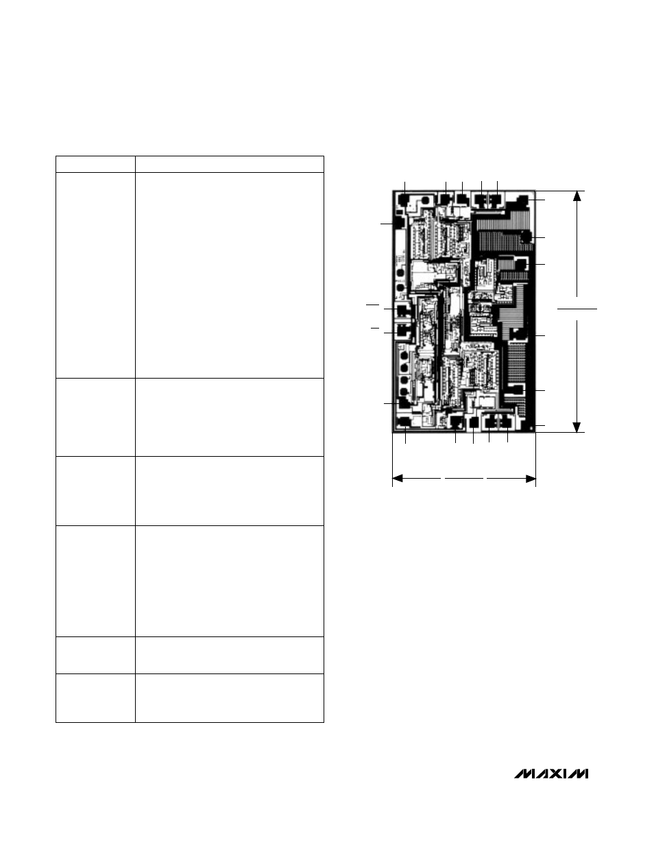
___________________Chip Topography
GND
EXT+
V+
EXT-
AV+
PUMP
PDRV
12/15
100/200
VREF
AGND
CC+ FB+ CSH+ CSL+
CSH-
CSL-
CC-
SS
FB-
0.135"
(3.45mm)
0.080"
(2.03mm)
TRANSISTOR COUNT: 375
SUBSTRATE CONNECTED TO V+
SYMPTOM
CORRECTION
Output is unloaded. Apply ±30mA or
greater load to observe waveform.
No Switching.
±VO are correct,
but no waveform is
seen at LX+ or LX-.
A. Check connections. VREF should be +2V.
B. When input voltage is less than +4.2V,
undervoltage lockout is enabled.
No Output.
+VO
= 5V or less. -VO
= 0V.
A. Inductor saturation: Peak currents
exceed coil ratings.
B. MOSFET on-resistance too high.
C. Switching losses: Diode is slow or has high
forward voltage. Inductor has high DC resis-
tance. Excess capacitance at LX nodes.
D. Inductor core losses: Hysteresis losses
cause self-heating in some core materials.
E. Loop instability: See
Unstable Output
above.
Poor Efficiency.
Supply current is
high. Output will
not drive heavy
loads.
A. Input overvoltage: Never apply more
than +12V.
B. FB+ or FB- disconnected or shorted. This
causes runaway and output overvoltage.
C. CC+ or CC- shorted.
D. Output filter capacitor disconnected.
Self-Destruction.
Transistors or IC
die on power-up.
A. Ground noise: Probe ground is picking up
switching EMI. Reduce probe ground lead
length (use probe tip shield) or put circuit
in shielded enclosure.
B. Poor HF response: Add ceramic or
tantalum capacitors in parallel with output
filter capacitors.
Noisy Output.
Switching is
steady, but large
inductive spikes
are seen at the
outputs.
Loop stability problem.
A. CC+ or CC- disconnected.
B. EMI: Move inductor away from IC or use
shielded inductors. Keep noise sources
away from CC- and CC+.
C. Grounding: Tie AGND directly to the filter
capacitor ground lead. Ensure that cur-
rent spikes from GND do not cause noise
at AGND or compensation capacitor or
reference bypass ground leads. Use wide
PC traces or a ground plane.
D. Bypass: Tie 10µF or larger between AGND
and VREF. Use 150µF to bypass the input
right at AV+. If there is high source resis-
tance, 1000µF or more may be required.
E. Current limiting: Reduce load currents.
Ensure that inductors are not saturating.
F. Slope compensation: Inductor value not
matched to sense resistor.
Unstable Output.
Noise or jitter on
output ripple
waveform. Scope
may not trigger
correctly.