Analog considerations, Reference and input, Bypassing – Rainbow Electronics MAX158 User Manual
Page 8
MAX154/MAX158
_____________Analog Considerations
Reference and Input
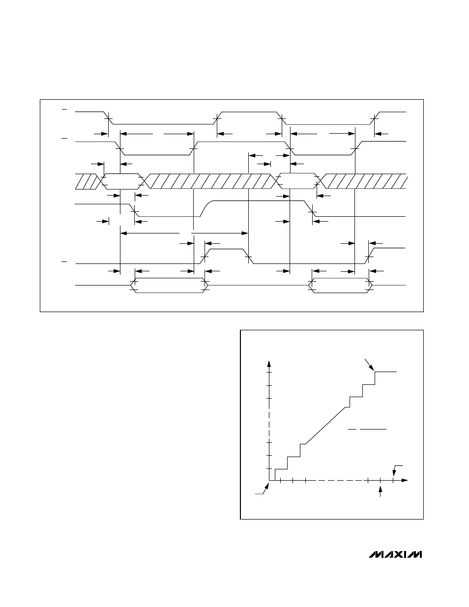
The V
REF
+ and V
REF
- inputs of the converter define the
zero and the full-scale of the ADC. In other words, the
voltage at V
REF
- is equal to the input voltage that pro-
duces an output code of all zeros, and the voltage at
V
REF
+ is equal to input voltage that produces an output
code of all ones (Figure 7).
Figure 8 shows some possible reference configura-
tions. A 0.01µF bypass capacitor to GND should be
used to reduce the high-frequency output impedance
of the internal reference. Larger capacitors should not
be used, as this degrades the stability of the reference
buffer. The 2.5V reference output is with respect to the
GND pin.
Bypassing
A 47µF electrolytic and 0.1µF ceramic capacitor should
be used to bypass the V
DD
pin to GND. These capaci-
tors must have minimum lead length, since excess lead
length may contribute to conversion errors and insta-
bility. If the reference inputs are driven by long lines,
they should be bypassed to GND with 0.1µF capac-
itors at the reference input pins.
CMOS High-Speed 8-Bit ADCs with
Multiplexer and Reference
8
_______________________________________________________________________________________
DATA
NEW
DATA
ADDR
VALID
INT
RDY
RD
ANALOG
CHANNEL
ADDRESS
CS
t
AS
t
AH
t
RDY
t
ACCI
t
CRD
t
RD
t
CSS
t
RD
t
RDY
t
INTH
t
DH
t
AH
t
INTH
t
AS
t
P
t
CSS
t
CSH
ADDR
VALID
OLD
DATA
t
DH
t
CSH
t
ACCI
Figure 6. Mode 1 Timing Diagram
11111111
11111110
11111101
00000011
00000010
00000001
00000000
1
V
REF
-
2
3
FS
V
REF
+
FS–1LSB
OUTPUT
CODE
FULL-SCALE
TRANSITION
1LSB = F8 = V
REF
+ - V
REF
-
256 256
AIN INPUT VOLTAGE
(IN TERMS OF LSBs)
Figure 7. Transfer Function