Electrical characteristics (continued) – Rainbow Electronics MAX158 User Manual
Page 3
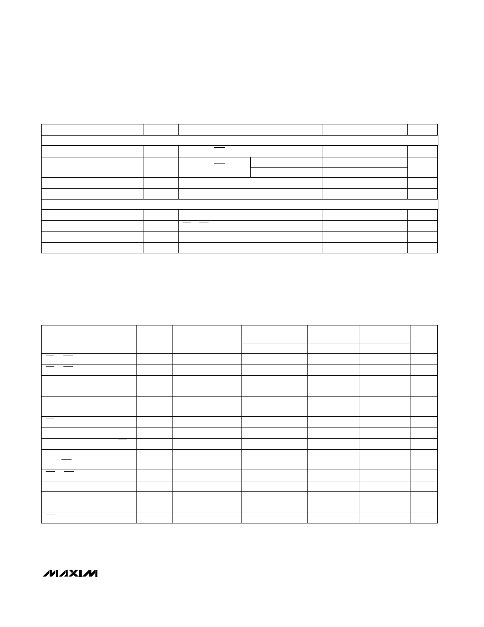
ELECTRICAL CHARACTERISTICS (continued)
(V
DD
= +5V, V
REF+
= +5V, V
REF-
= GND, MODE 0, T
A
= T
MIN
to T
MAX
, unless otherwise noted).
TIMING CHARACTERISTICS (Note 5)
(V
DD
= +5V, V
REF+
= +5V, V
REF-
= GND, MODE 0, T
A
= T
MIN
to T
MAX
, unless otherwise noted).
Note 5:
All input control signals are specified with t
R
= t
F
= 20ns (10% to 90% of +5V) and timed from a 1.6V voltage level.
Note 6:
Measured with load circuits of Figure 1 and defined as the time required for an output to cross 0.8V or 2.4V.
Note 7:
Defined as the time required for the data lines to change 0.5V when loaded with the circuits of Figure 2.
MAX154/MAX158
CMOS High-Speed 8-Bit ADCs with
Multiplexer and Reference
_______________________________________________________________________________________
3
(Note 6)
(Note 6)
C
L
= 50pF, R
L
= 5k
Ω
(Note 7)
C
L
= 50pF
CONDITIONS
ns
60
t
DH
Data Hold Time
ns
40
75
t
INTH
RD to INT Delay (Mode 1)
ns
0
t
CSH
ns
0
t
CSS
CS to RD Setup Time
CS to RD Hold Time
ns
20
50
t
ACC2
Data Access Time
After INT, Mode 0
ns
85
t
ACC1
Data Access Time After RD
µs
1.6
2.0
t
CRD
Conversion Time (Mode 0)
ns
30
40
t
RDY
CS to RDY Delay
ns
0
t
AS
Multiplexer Address
Setup Time
ns
30
t
AH
Multiplexer Address
Hold Time
UNITS
MIN
TYP
MAX
SYMBOL
ns
500
t
P
Delay Time
Between Conversions
500
70
100
0
0
60
110
2.4
60
0
35
MAX15_C/E
600
70
100
0
0
70
120
2.8
60
0
40
MAX15_M
MIN
MAX
MIN
MAX
ns
60
600
t
RD
RD Pulse Width (Mode 1)
80
500
80
400
DB0-DB7, INT; I
OUT
= -360µA
CS = RD = 2.4V
5V ±5% for specified performance
DB0-DB7, INT; RDY
DB0-DB7, RDY; V
OUT
= 0V to V
DD
V
DD
= ±5%
CONDITIONS
LSB
±1/16
±1/4
PSS
Power-Supply Sensitivity
V
4.0
V
OH
Output High Voltage
mW
25
75
Power Dissipation
mA
15
I
DD
Supply Current
V
4.75
5.25
V
DD
Supply Voltage
0.4
V
0.4
V
OL
Output Low Voltage
µA
±3
Three-State Output Current
pF
5
8
C
OUT
Output Capacitance (Note 4)
UNITS
MIN
TYP
MAX
SYMBOL
PARAMETER
I
OUT
= 1.6mA
I
OUT
= 2.6mA
LOGIC OUTPUTS
POWER-SUPPLY
PARAMETER
T
A
= +25°C
Note 1:
Total unadjusted error includes offset, full-scale, and linearity errors.
Note 2:
Specified with no external load unless otherwise noted.
Note 3:
Temperature drift is defined as change in output voltage from +25°C to T
MIN
or T
MAX
divided by (25 - T
MIN
) or (T
MAX
- 25).
Note 4:
Guaranteed by design.