Max1790, Low-noise step-up dc-dc converter, Chip information – Rainbow Electronics MAX1790 User Manual
Page 10: Layout procedure
MAX1790
for secondary outputs (V2 and V3) depends on the load
characteristics of all three outputs.
Layout Procedure
Good PC board layout and routing are required in high-
frequency switching power supplies to achieve good
regulation, high efficiency, and stability. It is strongly
recommended that the evaluation kit PC board layouts
be followed as closely as possible. Place power com-
ponents as close together as possible, keeping their
traces short, direct, and wide. Avoid interconnecting
the ground pins of the power components using vias
through an internal ground plane. Instead, keep the
power components close together and route them in a
“star” ground configuration using component-side
coper, then connect the star ground to internal ground
using multiple vias.
Chip Information
TRANSISTOR COUNT: 1012
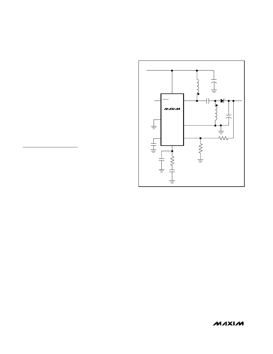
Low-Noise Step-Up DC-DC Converter
10
______________________________________________________________________________________
LX
IN
V
IN
2.6V TO 5.5V
GND
L1 = CTX8-1P
C
OUT
= TPSD226025R0200
C2
10
µF
FREQ
V
OUT
3.3V
CC
SS
SHDN
FB
D1
R1
1M
R2
605k
L1A
5.3
µH
0.027
µF
MAX1790
C
OUT
22
µF
20V
C1
10
µF
10V
R
COMP
22k
C
COMP
330pF
C
COMP2
56pF
L1B
5.3
µH
Figure 3. MAX1790 in a SEPIC Configuration