Detailed description – Rainbow Electronics MAX1419 User Manual
Page 9
MAX1419
15-Bit, 65Msps ADC with -79.3dBFS
Noise Floor for Baseband Applications
_______________________________________________________________________________________
9
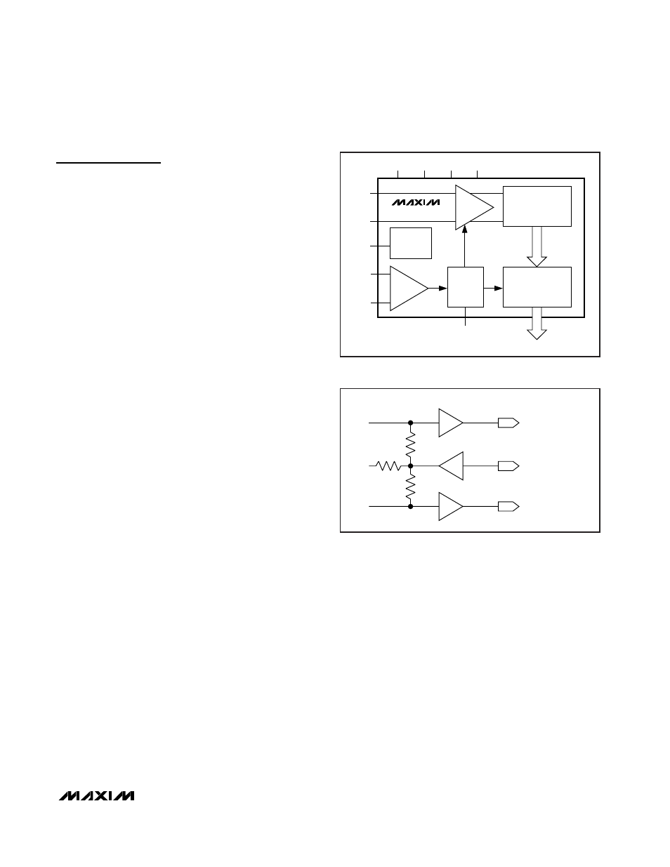
Detailed Description
Figure 1 provides an overview of the MAX1419 archi-
tecture. The MAX1419 employs an input T/H amplifier,
which has been optimized for low thermal noise and
low distortion. The high-impedance differential inputs to
the T/H amplifier (INP and INN) are self-biased at
3.38V, and support a full-scale differential input voltage
of 2.56V
P-P
. The output of the T/H amplifier is fed to a
multistage pipelined ADC core, which has also been
optimized to achieve a very low thermal noise floor and
low distortion.
A clock buffer receives a differential input clock wave-
form and generates a low-jitter clock signal for the input
T/H. The signal at the analog inputs is sampled at the
rising edge of the differential clock waveform. The dif-
ferential clock inputs (CLKP and CLKN) are high-
impedance inputs, are self-biased at 2.4V, and support
differential clock waveforms from 0.5V
P-P
to 3.0V
P-P
.
The outputs from the multistage pipelined ADC core
are delivered to error correction and formatting logic-
which in turn, deliver the 15-bit output code in two’s-
complement format to digital output drivers. The output
drivers provide CMOS-compatible outputs with levels
programmable over a 2.3V to 3.5V range.
Analog Inputs and
Common Mode (INP, INN, CM)
The signal inputs to the MAX1419 (INP and INN) are
balanced differential inputs. This differential configura-
tion provides immunity to common-mode noise coupling
and rejection of even-order harmonic terms. The differ-
ential signal inputs to the MAX1419 should be AC-cou-
pled and carefully balanced in order to achieve the best
dynamic performance (see the Applications Information
section for more detail). AC-coupling of the input signal
is easily accomplished because the MAX1419 inputs
are self-biasing as illustrated in Figure 2. Although the
T/H inputs are high impedance, the actual differential
input impedance is nominally 1kΩ because of the two
500Ω bias resistors connected from each input to the
common-mode reference.
The CM pin provides a monitor of the input common-
mode self-bias potential. In most applications, in which
the input signal is AC-coupled, this pin is not connect-
ed. If DC-coupling of the input signal is required, this
pin may be used to construct a DC servo loop to con-
trol the input common-mode potential. See the
Applications Information section for more details.
T/H
CORRECTION
LOGIC + OUTPUT
BUFFERS
INTERNAL
TIMING
INTERNAL
REFERENCE
INP
INN
CM
CLKP
CLKN
DAV
15
DATA BITS D0 THROUGH D14
AV
CC
DRV
CC
DV
CC
GND
MULTISTAGE
PIPELINE ADC CORE
CLOCK
BUFFER
MAX1419
Figure 1. Simplified MAX1419 Block Diagram
BUFFER
INTERNAL REFERENCE
AND BIASING CIRCUIT
T/H AMPLIFIER
T/H AMPLIFIER
500Ω
500Ω
CM
INP
INN
TO 1. QUANTIZER STAGE
TO 1. QUANTIZER STAGE
1kΩ
Figure 2. Simplified Analog and Common-Mode Input Architecture