Rainbow Electronics MAX754 User Manual
Page 2
MAX753/MAX754
CCFL Backlight and
LCD Contrast Controllers
2
_______________________________________________________________________________________
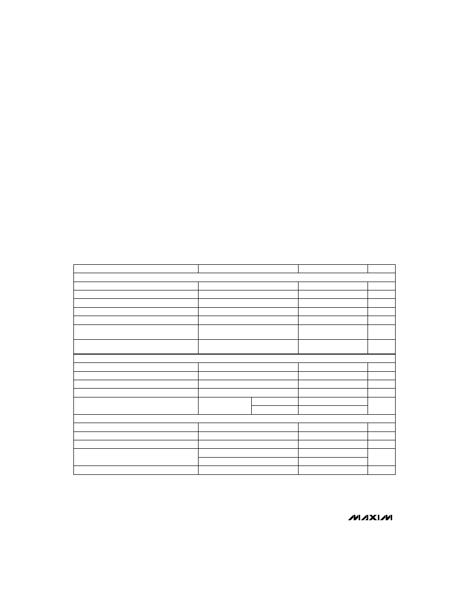
ABSOLUTE MAXIMUM RATINGS
ELECTRICAL CHARACTERISTICS
(V
DD
= 5V, BATT = 15V, CON = LON = 5V, LX = GND = PGND = 0V, I
REF
= 0mA, all digital input levels are 0V or 5V,
T
A
= T
MIN
to T
MAX
, unless otherwise noted.)
Stresses beyond those listed under “Absolute Maximum Ratings” may cause permanent damage to the device. These are stress ratings only, and functional
operation of the device at these or any other conditions beyond those indicated in the operational sections of the specifications is not implied. Exposure to
absolute maximum rating conditions for extended periods may affect device reliability.
V
DD
to GND .................................................................-0.3V, +7V
PGND to GND.....................................................................±0.3V
BATT to GND.............................................................-0.3V, +36V
LX to GND............................................................................±50V
CS to GND.....................................................-0.6V, (V
DD
+ 0.3V)
Inputs/Outputs to GND (LADJ, CADJ, LON,
CON, REF, CFB, CC, CDRV, LDRV, LFB) .....-0.3V, (V
DD
+ 0.3V)
Continuous Power Dissipation (T
A
= +70°C)
Plastic DIP (derate 10.53mW/°C above +70°C) ...........842mW
Narrow SO (derate 8.70mW/°C above +70°C) .............696mW
Operating Temperature Ranges
MAX75_C_ _ ........................................................0°C to +70°C
MAX75_E_ _......................................................-40°C to +85°C
Junction Temperature ......................................................+150°C
Storage Temperature Range .............................-65°C to +160°C
Lead Temperature (soldering, 10sec) .............................+300°C
Guaranteed monotonic
Maximum, CFB = 0V
Minimum, CFB = 5V
V
CS
= 0V
LON, CON, CADJ, LADJ; V
DD
= 5.5V
LON, CON, CADJ, LADJ; V
DD
= 4.5V
LDRV, CDRV;
V
DD
= 4.5V
No external load
4V < V
DD
< 6V
0µA < I
L
< 100µA
LDRV = CDRV = 2V
LON, CON, CADJ, LADJ; V
IN
= 0V or 5V
CONDITIONS
Bits
5
DAC Resolution
85
115
kHz
32
47
VCO Frequency
µA
-5
CS Input Bias Current
V
1.2
1.3
Overcurrent-Comparator Threshold Voltage (CS)
mV
-10
20
Zero-Crossing-Comparator Threshold Voltage (CS)
7
Ω
10
Driver On-Resistance
A
0.5
Driver Sink/Source Current
µA
±1
Input Leakage Current
V
4.5
5.5
V
DD
Supply Range
V
4
30
BATT Input Range
V
2.4
Input High Voltage
V
0.8
Input Low Voltage
µA
25
40
V
DD
Shutdown Current
V
1.21
1.25
1.29
REF Output Voltage
%/V
0.1
REF Line Regulation
mV
5
15
REF Load Regulation
mA
0.5
2
V
DD
Quiescent Current
UNITS
MIN
TYP
MAX
PARAMETER
LON = CON = CS = LFB = CFB =
LADJ = CADJ = 5V
Output high
Output low
LON = CON = CS = LFB = CFB = LADJ
= CADJ = LX = BATT = 0V (Note 1)
SUPPLY AND REFERENCE
DIGITAL INPUTS AND DRIVER OUTPUTS
CCFT CONTROLLER