Pin description, Detailed description – Rainbow Electronics MAX853 User Manual
Page 6
MAX850–MAX853
Low-Noise, Regulated, Negative
Charge-Pump Power Supplies for GaAsFET Bias
6
______________________________________________________________________________________
______________________________________________________________Pin Description
MAX850
MAX851
MAX852
-1.28V
REF
CHARGE
PUMP
IN
N
C1+
C1-
NEGOUT
SHDN (MAX850)
SHDN (MAX851)
OSC (MAX852)
OUT
CONNECT TO
GND TO SET
V
OUT
= -4.1V
FB
GND
MAX853
CHARGE
PUMP
IN
N
C1+
C1-
NEGOUT
SHDN
OUT
CONTROL
VOLTAGE
CONT
GND
_______________Detailed Description
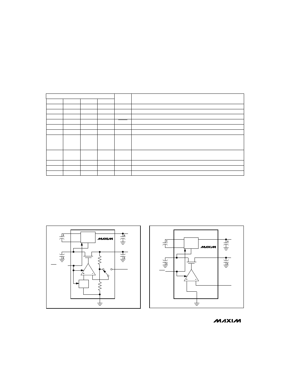
The MAX850–MAX853 are low-noise, inverting, regulat-
ed charge-pump power supplies designed for biasing
GaAsFET devices, such as power-amplifier modules in
cellular handsets.
The applied input voltage (V
IN
) is first inverted to a
negative voltage at NEGOUT by a capacitive charge
pump. This voltage is then regulated by an internal lin-
ear regulator, and appears at OUT (Figure 1). The mini-
mum (most negative) output voltage (V
OUT
) achievable
is the inverted positive voltage, plus the 1.0V required
by the post-regulator. The ripple noise induced by the
charge-pump inverter is reduced by the linear regulator
to 2mVp-p at V
OUT
for the MAX850–MAX852. In addi-
tion, the excellent AC rejection of the linear regulator
attenuates noise on the incoming supply. Up to 5mA is
available at OUT.
Figure 1a. MAX850–MAX852 Block Diagram
Figure 1b. MAX853 Block Diagram
MAX850
1
MAX851
1
MAX853
1
PIN
MAX852
1
NAME
C1+
FUNCTION
Positive terminal for C1
3
–
2
3
3
4
2
3
–
2
4
NEGOUT
SHDN
2
C1-
Negative Output Voltage (unregulated), V
NEGOUT
= V
IN
+ 0.2V
Active-low TTL logic level Shutdown Input
Negative terminal for C1
–
4
–
–
–
4
–
OSC
–
SHDN
External Clock Input
Active-high TTL logic level Shutdown Input
5
5
–
5
FB
Dual-Mode Feedback Input. When FB is grounded, the output is preset to
-4.1V. To select other output voltages, connect FB to an external resistor
divider. See Figure 2b.
–
5
–
–
CONT
Control Voltage Input. To set V
OUT
, connect a resistor divider between
OUT and a positive control voltage between 0V and 10V. See Figure 2c.
7
8
6
7
7
8
6
7
8
6
8
GND
IN
6
OUT
Ground
Positive Power-Supply Input (4.5V to 10V)
Output Voltage