Design procedure, Chip information, Table 1. external component selection – Rainbow Electronics MAX679 User Manual
Page 6: Table 2. manufacturers of low-esr capacitors
Maxim cannot assume responsibility for use of any circuitry other than circuitry entirely embodied in a Maxim product. No circuit patent licenses are
implied. Maxim reserves the right to change the circuitry and specifications without notice at any time.
6
___________________Maxim Integrated Products, 120 San Gabriel Drive, Sunnyvale, CA 94086 (408) 737-7600
© 1997 Maxim Integrated Products
Printed USA
is a registered trademark of Maxim Integrated Products.
MAX679
Regulated 3.3V Charge Pump
Maxim cannot assume responsibility for use of any circuitry other than circuitry entirely embodied in a Maxim product. No circuit patent licenses are
implied. Maxim reserves the right to change the circuitry and specifications without notice at any time.
6
___________________Maxim Integrated Products, 120 San Gabriel Drive, Sunnyvale, CA 94086 (408) 737-7600
© 1997 Maxim Integrated Products
Printed USA
is a registered trademark of Maxim Integrated Products.
cycles (about 4ms) have elapsed. The start-up
sequence begins at power-up, when exiting shutdown,
or when recovering from a short circuit. If V
IN
is less
than the 1.6V UVLO threshold, the device remains shut
down and ignores a high SHDN input.
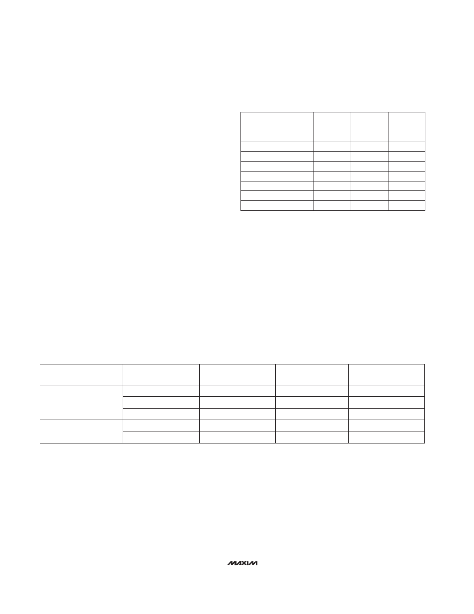
__________________Design Procedure
Optimize the charge-pump circuit for size, quiescent
current, and output ripple by properly selecting the
operating frequency and capacitors C
IN
, C1, and
C
OUT
.
For lowest output ripple, select 1MHz operation (FSET
= IN). In addition, increasing C
OUT
relative to C1 will
further reduce ripple. For highest efficiency, select
330kHz operation (FSET = GND) and select the largest
practical values for C
OUT
and C1 while maintaining a
30-to-1 ratio. See Table 1 for some suggested values
and the resulting output ripple.
Note that the capacitors must have low ESR (<20m
Ω
)
to maintain low ripple. Currently, only ceramic capaci-
tors can provide such low ESR; therefore, the output fil-
ter capacitors should be a combination of a 1µF
ceramic capacitor and a 10µF tantalum capacitor.
Smallest Size
Set the frequency to 1MHz by connecting FSET to IN.
Table 1 shows typical external component values.
Table 1. External Component Selection
PC Board Layout
Place C1, C
OUT
, and C
IN
close to the IC. Connect
PGND and GND with a short trace.
Efficiency
Charge-pump efficiency is best at low frequency
(330kHz). The theoretical maximum efficiency is given
in the following equation:
Theoretical maximum efficiency = V
OUT
/ (2 x V
IN
)
Gate-charge losses amount to approximately 1mA from
the output at full switching frequency (about 5% to 7%
loss).
Table 2. Manufacturers of Low-ESR Capacitors
TRANSISTOR COUNT: 819
SUBSTRATE CONNECTED TO GND
___________________Chip Information
C1
(µF)
C
OUT
(µF)
2
0.33
10
10
FSET
(Hz)
Vp-p
(mV)
V
IN
(V)
1M
7
14
330k
2
0.33
2
0.1
3.3
3.3
1M
16
22
330k
2
0.1
3
0.33
10
10
1M
27
56
330k
3
0.33
3
0.1
3.3
3.3
1M
72
89
330k
3
0.1
X7R
(714) 960-6492
(714) 969-2491
Surface-Mount
Ceramic Capacitors
Matsuo
Sprague
593D, 595D series
X7R
(603) 224-1961
(603) 224-1430
(803) 626-3123
(803) 946-0690
AVX
MANUFACTURER
CAPACITORS
Surface-Mount
Tantalum Capacitors
AVX
TPS series
267 series
PHONE
FAX
PRODUCTION
METHOD
(803) 946-0690
(803) 626-3123
(714) 960-6492
(714) 969-2491
Matsuo