Typical operating characteristics (continued), Pin description, Detailed description – Rainbow Electronics MAX679 User Manual
Page 4: Start-up sequence
MAX679
Regulated 3.3V Charge Pump
4
_______________________________________________________________________________________
____________________________Typical Operating Characteristics (continued)
(Typical Operating Circuit with: V
IN
= V
S HDN
= 2V, C
IN
= 4.7µF, C1 = 0.33µF, C
OUT
= 10µF, tested in-circuit, T
A
= +25°C, unless
otherwise noted.)
______________________________________________________________Pin Description
NAME
FUNCTION
1
FSET
Set Charge-Pump Frequency Input. FSET = GND selects 330kHz and FSET = IN selects 1MHz. Do not leave
FSET unconnected.
2
SHDN
Shutdown Input. The device shuts down, the output disconnects from the input, and the supply current
decreases to 1µA when SHDN is a logic low. Connect SHDN to IN for normal operation.
PIN
3
IN
Supply Input. Connect to an input supply in the 1.8V to 3.6V range. Bypass IN to GND with a (C
OUT
/ 2)µF
capacitor.
4
GND
Ground. Analog ground for internal reference and control circuitry.
8
OUT
3.3V Power Output. Bypass OUT to GND with an output filter capacitor (see the
Design Procedure
section).
7
C1+
Positive Terminal of the Charge-Pump Capacitor
6
C1-
Negative Terminal of the Charge-Pump Capacitor
5
PGND
Power Ground. Charge-pump current flows through this pin.
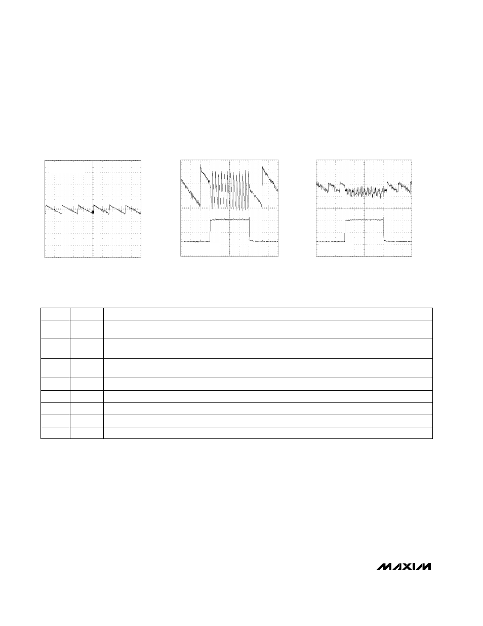
LOAD-TRANSIENT RESPONSE
(1mA TO 10mA LOAD, V
IN
= 3V)
MAX679 TOC11
V
OUT
10mV/div
AC COUPLED
I
OUT
5mA/div
100
µ
s/div
V
IN
= 3V
FSET = IN (1MHz)
LOAD-TRANSIENT RESPONSE
(1mA TO 10mA LOAD, V
IN
= 2V)
MAX679 TOC12
V
OUT
10mV/div
AC COUPLED
I
OUT
5mA/div
50
µ
s/div
V
IN
= 2V
FSET = IN (1MHz)
_______________Detailed Description
The MAX679 regulated charge pump has a 50% duty-
cycle clock. In phase one (charge phase), the charge-
transfer capacitor (C1) charges to the input voltage,
and output current is delivered by the output filter
capacitor (C
OUT
). In phase two (transfer phase), C1 is
placed in series with the input and connects to the out-
put, transferring its charge to C
OUT
. If the clock were to
run continuously, this process would eventually gener-
ate an output voltage equal to two times the input volt-
age (hence the name “doubler”).
The charge pump regulates by gating the oscillator on
and off as needed to maintain output regulation. This
method has low quiescent current, but to achieve
acceptable output ripple, C1 must be significantly
lower in value than C
OUT
.
Start-Up Sequence
The MAX679 soft-start circuitry prevents excessive cur-
rent from being drawn from the battery at start-up or
when the output is shorted. This is done by limiting the
charge pump to 1/10 the normal current until either the
output is in regulation or the first 4096 charge-pump
OUTPUT RIPPLE (2mA LOAD)
MAX679 TOC10
V
OUT
50mV/div
AC COUPLED
100
µ
s/div
FSET = IN (1MHz)