Applications information – Rainbow Electronics MAX1708 User Manual
Page 12
MAX1708
High-Frequency, High-Power, Low-Noise,
Step-Up DC-DC Converter
12
______________________________________________________________________________________
Diode Selection (D1)
The MAX1708’s high switching frequency demands a
high-speed rectifier. Use Schottky diodes (Table 3).
The diode’s current rating must exceed the maximum
load current, and its breakdown voltage must exceed
V
OUT
. The diode must be placed within 10mm of the
LX switching node and the output filter capacitor. The
diode also must be able to dissipate the power calcu-
lated by the following equation:
P
DIODE
= I
OUT
✕
V
D
where I
OUT
is the average load current and V
D
is the
diode forward voltage at the peak switch current.
Capacitor Selection
Input Bypass Capacitor (C1)
A 150µF, low-ESR input capacitor will reduce peak cur-
rents and reflected noise due to inductor current ripple.
Lower ESR allows for lower input ripple current, but
combined ESR values up to 100m
Ω are acceptable.
Smaller ceramic capacitors may also be used for light
loads or in applications that can tolerate higher input
current ripple.
Output Filter Capacitor (C2)
The output filter capacitor ESR must be kept under
30m
Ω for stable operation. Polymer capacitors of
150µF (Panasonic EEFUE0J151R) typically exhibit
10m
Ω of ESR. This translates to approximately 35mV of
output ripple at 3.5A switch current. Bypass the
MAX1708 IC supply input (OUT) with a 0.1µF ceramic
capacitor to GND and a 2
Ω series resistor (R2, as
shown in Figure 1).
MAX1708 IC Power Dissipation
The major components of MAX1708 dissipated power
are switch conductance loss (P
SW
), capacitive loss
(P
CAP
), and switch transition loss (P
TRAN
). Numerical
examples provided in brackets ({ }) correspond to the
following condition:
{V
IN
= 3.3V, V
OUT
= 5V, V
D
= 0.5V, I
OUT
= 2A}
An important parameter to compute the power dissipat-
ed in the MAX1708 is the approximate peak switch cur-
rent (I
SW
):
P
D
= P
SW
+ P
CAP
+ P
TRAN
{0.472W}
P
SW
= (1 - D') I
SW
2 ✕
R
SW
{0.353W}
P
CAP
= (C
DIO
+ C
DSW
+ C
GSW
) (V
OUT
+ V
D
)
2
f {0.045W}
P
TRAN
= (V
OUT
+ V
D
) I
SW
✕
t
SW
✕
f / 3 {0.073W}
where:
R
SW
= switch resistance {80m
Ω}
C
DIO
= catch-diode capacitance {500pF}
C
DSW
= switch drain capacitance {1250pF}
C
GSW
= switch gate capacitance {750pF}
f = switching frequency {600kHz}
t
SW
= switch turn-on or turn-off time {20ns}
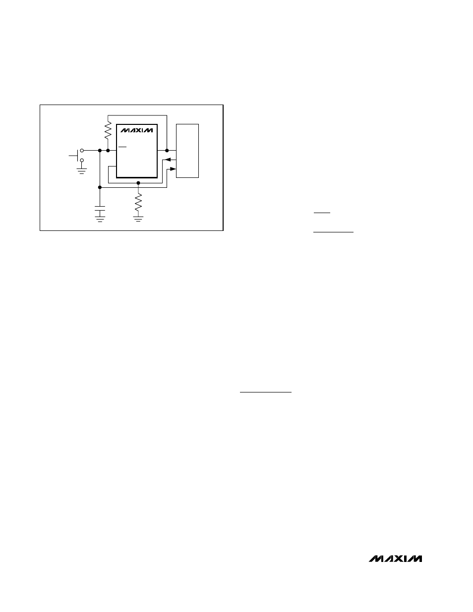
Applications Information
Using a Momentary On/Off Switch
A momentary pushbutton switch can be used to turn
the MAX1708 on and off. As shown in Figure 5, when
ONA is pulled low and ONB is pulled high, the device
is off. When the momentary switch is pressed, ONB is
pulled low and the regulator turns on. The switch
should be on long enough for the microcontroller to exit
reset. The controller issues a logic high to ONA, which
guarantees that the device will stay on regardless of
the subsequent switch state. To turn the regulator off,
depress the switch long enough for the controller to
read the switch status and pull ONA low. When the
switch is released, ONB pulls high and the regulator
turns off.
Layout Considerations
Due to high inductor current levels and fast switching
waveforms, proper PC board layout is essential. Protect
I
I
D
A
D
V
V
V
SW
OUT
IN
OUT
D
'
{ .
}
'
{ . }
=
=
+
3 33
0 6
µC
270k
Ω
ONB
ONA
0.1
µF
270k
Ω
ON/OFF
MAX1708
V
DD
I/O
I/O
Figure 5. Momentary Pushbutton On-Off Switch