Detailed description, Pin description (continued) – Rainbow Electronics MAX1779 User Manual
Page 9
MAX1779
Low-Power Triple-Output TFT LCD DC-DC
Converter
_______________________________________________________________________________________
9
Detailed Description
The MAX1779 is a highly efficient triple-output power
supply for TFT LCD applications. The device contains
one high-power step-up converter and two low-power
charge pumps. The primary boost converter uses an
internal N-channel MOSFET to provide maximum effi-
ciency and to minimize the number of external compo-
nents. The output voltage of the main boost converter
(V
MAIN
) can be set from V
IN
to 13V with external resistors.
The dual charge pumps independently regulate a posi-
tive output (V
POS
) and a negative output (V
NEG
). These
low-power outputs use external diode and capacitor
stages (as many stages as required) to regulate output
voltages up to +40V and down to -40V. A proprietary
regulation algorithm minimizes output ripple as well as
capacitor sizes for both charge pumps.
Also included in the MAX1779 are a precision 1.25V
reference that sources up to 50µA, logic shutdown,
soft-start, power-up sequencing, fault detection, and an
active-low open-drain ready output.
Main Boost Converter
The MAX1779 main step-up converter switches at a
constant 250kHz internal oscillator frequency to allow
the use of small inductors and output capacitors. The
MOSFET switch pulse width is modulated to control the
power transferred on each switching cycle and to regu-
late the output voltage.
During PWM operation, the internal clock’s rising edge
sets a flip-flop, which turns on the N-channel MOSFET
(Figure 1). The switch turns off when the voltage-error,
slope-compensation, and current-feedback signals trip
the comparators and reset the flip-flop. The switch
remains off for the rest of the clock cycle. Changes in
the output voltage error signal shift the switch current
trip level, consequently modulating the MOSFET duty
cycle.
Dual Charge-Pump Regulator
The MAX1779 contains two individual low-power charge
pumps. One charge pump inverts the supply voltage
(SUPN) and provides a regulated negative output voltage.
The second charge pump doubles the supply voltage
(SUPP) and provides a regulated positive output voltage.
The MAX1779 contains internal P-channel and N-channel
MOSFETs to control the power transfer. The internal
MOSFETs switch at a constant 125kHz (0.5
✕
f
OSC
).
Negative Charge Pump
During the first half-cycle, the P-channel MOSFET turns
on and the flying capacitor C5 charges to V
SUPN
minus
a diode drop (Figure 2). During the second half-cycle,
the P-channel MOSFET turns off, and the N-channel
MOSFET turns on, level shifting C5. This connects C5 in
parallel with the reservoir capacitor C6. If the voltage
across C6 minus a diode drop is lower than the voltage
across C5, charge flows from C5 to C6 until the diode
(D5) turns off. The amount of charge transferred to the
output is controlled by the variable N-channel on-resis-
tance.
Positive Charge Pump
During the first half-cycle, the N-channel MOSFET turns
on and charges the flying capacitor C3 (Figure 3). This
initial charge is controlled by the variable N-channel
on-resistance. During the second half-cycle, the N-
channel MOSFET turns off and the P-channel MOSFET
turns on, level shifting C3 by V
SUPP
volts. This connects
C3 in parallel with the reservoir capacitor C4. If the volt-
age across C4 plus a diode drop (V
POS
+ V
DIODE
) is
smaller than the level-shifted flying capacitor voltage
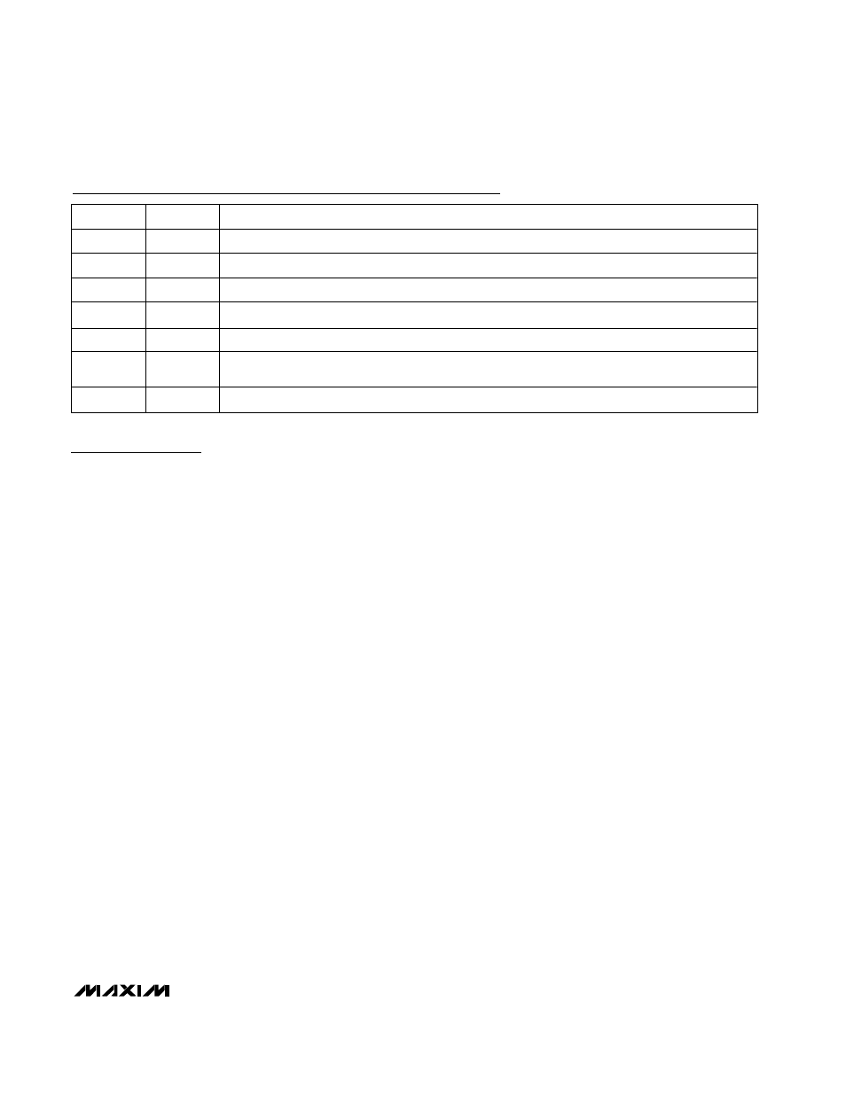
Pin Description (continued)
PIN
NAME
FUNCTION
10
DRVN
Negative Charge-Pump Driver Output. Output high level is V
SUPN
, and low level is PGND.
11
SUPN
Negative Charge-Pump Driver Supply Voltage. Bypass to PGND with a 0.1
µF capacitor.
12
DRVP
Positive Charge-Pump Driver Output. Output high level is V
SUPP
, and low level is PGND.
13
SUPP
Positive Charge-Pump Driver Supply Voltage. Bypass to PGND with a 0.1
µF capacitor.
14
PGND
Power Ground. Connect to GND underneath the IC.
15
LX
Main Boost Regulator Power MOSFET N-Channel Drain. Connect output diode and output capacitor
as close to PGND as possible.
16
TGND
Must be connected to ground.