Rainbow Electronics MAX1677 User Manual
Page 2
MAX1677
Compact, High-Efficiency, Dual-Output
Step-Up and LCD Bias DC-DC Converter
2
_______________________________________________________________________________________
ABSOLUTE MAXIMUM RATINGS
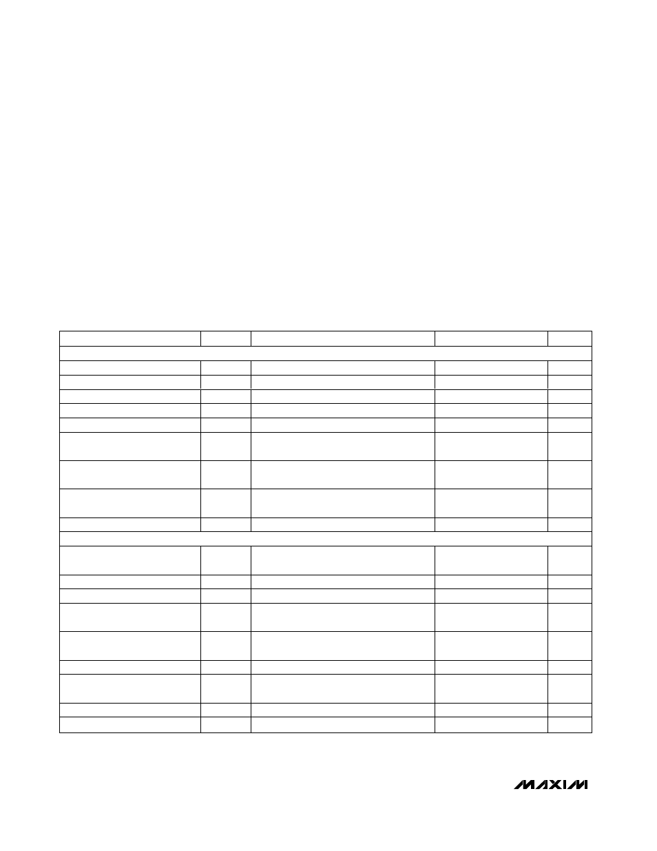
ELECTRICAL CHARACTERISTICS
(V
OUT
= 3.3V, C
REF
= 0.1µF, POUT = OUT, T
A
= 0°C to +85°C, unless otherwise noted. Typical values are at T
A
= +25°C.)
Stresses beyond those listed under "Absolute Maximum Ratings" may cause permanent damage to the device. These are stress ratings only, and functional
operation of the device at these or any other conditions beyond those indicated in the operational sections of the specifications is not implied. Exposure to
absolute maximum rating conditions for extended periods may affect device reliability.
OUT, LCDON, ON, POUT, LBI,
LBO,
LX to GND .............................................................-0.3V to +6V
CLK/SEL, LCDPOL, REF, LCDFB,
FB to GND .............................................-0.3V to (V
OUT
+ 0.3V)
LCDLX to GND .......................................................-0.3V to +30V
PGND, LCDGND to GND ......................................-0.3V to +0.3V
POUT to OUT.........................................................-0.3V to +0.3V
Continuous Power Dissipation (T
A
= +70°C)
16-Pin QSOP (derate 8.3mW/°C above +70°C)...........696mW
Operating Temperature Range ...........................-40°C to +85°C
Junction Temperature ......................................................+150°C
Storage Temperature Range .............................-65°C to +160°C
Lead Temperature (soldering, 10s) .................................+300°C
PARAMETER
SYMBOL
CONDITIONS
MIN
TYP
MAX
UNITS
GENERAL
Input Voltage Range
V
IN
(Note 1)
0.7
5.5
V
Minimum Startup Voltage
V
STARTUP
T
A
= +25°C, I
LOAD
< 1mA
0.9
1.1
V
Reference Voltage
V
REF
I
REF
= 0
1.23
1.25
1.27
V
Reference Load Regulation
I
REF
= 0 to 50µA (Note 2)
2
15
mV
Reference Line Rejection
V
OUT
= 2.5V to 5.5V
0.2
5
mV
Supply Current
Main DC On, LCD Off
I
LCDOFF
No load, current into OUT
20
40
µA
Supply Current All On,
Main DC-DC in PFM Mode
I
PFM
No load, current into OUT
35
60
µA
Supply Current All On,
Main DC-DC in PWM Mode
I
PWM
No load, current into OUT
115
300
µA
Supply Current in Shutdown
0.3
5
µA
MAIN BOOST DC-DC
Output Voltage
V
OUT
FB = GND, 0
≤ I
LX
≤ 350mA,
CLK/SEL = OUT (Note 3)
3.20
3.30
3.43
V
FB Regulation Voltage
V
FB (REG)
Adjustable mode, CLK/SEL = OUT (Note 3)
1.225
1.25
1.275
V
FB Input Current
I
FB
V
FB
= 1.3V
0.02
50
nA
Output Voltage Adjustment
Range
2.5
5.5
V
Startup to Normal Mode
Transition Voltage (Note 4)
V
LOCKOUT
2.1
2.4
V
Line Regulation
I
OUT
= 150mA, V
IN
= 2V to 3V
0.6
%
Load Regulation
CLK/SEL = OUT, V
IN
= 2.4V,
I
LOAD
= 10mA to 200mA
1
%
Frequency in Startup Mode
f
STARTUP
V
OUT
= 15V
40
300
kHz
LX Leakage Current
I
LX (LEAK)
0.2
5
µA