Applications information – Rainbow Electronics MAX1677 User Manual
Page 13
MAX1677
Compact, High-Efficiency, Dual-Output
Step-Up and LCD Bias DC-DC Converter
______________________________________________________________________________________
13
in the 10k
Ω to 200kΩ range and calculate R1 using one
of the following two equations (for positive or negative
output).
For a positive LCD output, connect LCDPOL to OUT as
shown in Figure 2. This sets the threshold at LCDFB to
1.25V. Select R2 and the desired output voltage
(V
LCD
), and calculate R1:
For positive LCD output: R1 = R2 [(V
LCD
/ 1.25V) - 1]
Figure 3 shows the standard circuit for generating a
negative LCD supply. This connection limits V
LCD
to
values between -V
IN
and -28V. If a smaller negative
output voltage is required, D2’s cathode can be con-
nected to V
IN
rather than ground. This alternate con-
nection permits output voltages from 0 to -
28 - V
IN
.
For a negative LCD output voltage, connect LCDPOL to
GND. The feedback threshold voltage of LCDFB is set
to 0. Select R2 and the desired output voltage (V
LCD
),
and calculate R1:
For negative LCD output: R1 = R2
×
V
LCD
/ 1.25V
To minimize ripple in the LCD output and prevent sub-
harmonic noise caused by switching pulse grouping, it
may be necessary in some PC board layouts to con-
nect a small capacitor in parallel with R1. For R1 values
in 500k
Ω to 2MΩ range, 22pF is usually adequate.
Many LCD bias applications require an adjustable out-
put voltage. In Figure 9, an external control voltage
(generated by a potentiometer, DAC, filtered PWM con-
trol signal, or other source) is coupled to LCDFB
through the resistor R
ADJ
. The output voltage of this cir-
cuit, for both positive and negative outputs, is given by:
V
OUT
= V
INIT
+ (R1 / R
ADJ
)(V
LCDFB
- V
ADJ
)
where V
INIT
is the initial output obtained without the
added adjust voltage, as calculated in one of the pre-
ceding two equations. V
LCDFB
is 1.25V for the positive
configuration, and 0 for the negative configuration.
R
ADJ
sets the output adjustment span, which is
1.25V
× R1 / R
ADJ
for either polarity output. Note that
raising V
ADJ
lowers V
OUT
in positive output designs,
while in negative output designs, raising V
ADJ
increas-
es the magnitude of the negative output.
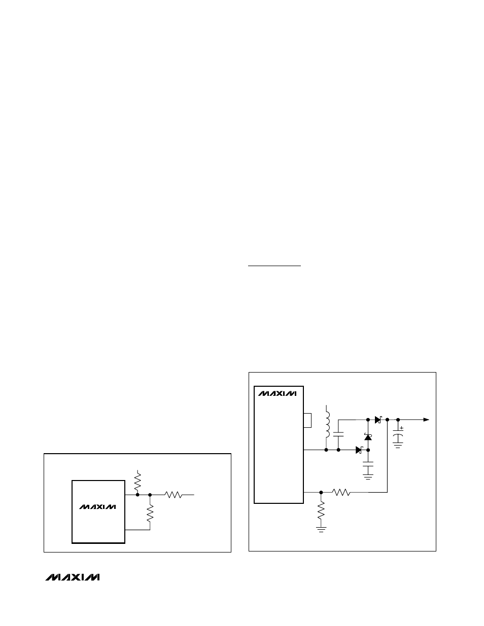
Higher LCD Output Voltages
If the application requires LCD output voltages greater
than +28V, use the connection in Figure 10. This circuit
adds one capacitor-diode charge pump stage to
increase the output voltage without increasing the volt-
age stress on the LCDLX pin. The maximum output
voltage of the circuit is +55V and output current is
slightly less than half that available from the standard
circuit in Figure 2. In Figure 10, diodes D1, D2, and D3
should be at least 30V-rated Schottky diodes such as
1N5818 or MBR0530L or equivalent. Capacitors C1
and C2 should also be rated for 30V, while C3 must be
rated for the maximum set output voltage.
Applications Information
Inductor Selection
The MAX1677’s high switching frequency allows the
use of small surface-mount inductors. The 10µH values
shown in Figures 2 and 3 are recommended for most
applications, although values between 4.7µH and 47µH
are suitable. Smaller inductance values typically offer a
smaller physical size for a given series resistance,
allowing the smallest overall circuit dimensions. Larger
inductance values exhibit higher output current capa-
bility, but larger physical dimensions.
MAX1677
FB
R2
R1
V
ADJ
R
ADJ
V
LCD
GND
(REF)
Figure 9. Adjusting LCD Output Voltage
MAX1677
LCDLX
OUT
LCDPOL
L2
10
µH
D1
D2
D3
C1
1
µF
30V
C2
2.2
µF
30V
C3
2.2
µF
+40V/5mA
(SET TO
NO MORE
THAN 55V)
D1, D2, D3 = 30V RATED SCHOTTKY DIODES:
MBR0530L OR EQUIVALENT.
R2
65k
R1
2M
1
7
12
10
V
IN
LCDFB
Figure 10. Higher LCD Output Voltage