Rainbow Electronics MAX1874 User Manual
Page 2
MAX1874
Dual-Input, USB/AC Adapter, 1-Cell
Li+ Charger with OVP and Thermal Regulation
2
_______________________________________________________________________________________
ABSOLUTE MAXIMUM RATINGS
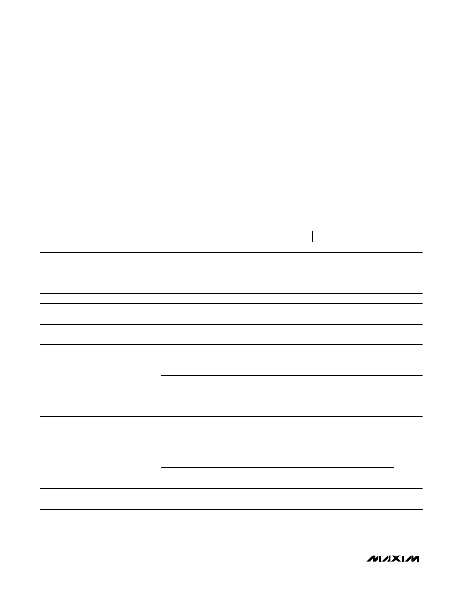
ELECTRICAL CHARACTERISTICS
(V
USB
= V
DC
= V
DCLV
= V
EN
= V
USEL
= 5V, V
BATT
= 4.2V, V
THRM
= V
REF
/ 2, Circuit of Figure 2, T
A
= 0°C to +85°C, unless otherwise
noted. Typical values are at T
A
= +25°C.)
Stresses beyond those listed under “Absolute Maximum Ratings” may cause permanent damage to the device. These are stress ratings only, and functional
operation of the device at these or any other conditions beyond those indicated in the operational sections of the specifications is not implied. Exposure to
absolute maximum rating conditions for extended periods may affect device reliability.
DC, DCOK to GND .................................................-0.3V to +20V
DCLV, BYP, USB, UOK, DCI, REF, USEL, THRM,
EN, BATT, CHG, PON to GND .............................-0.3V to +7V
PGND to GND .......................................................-0.3V to +0.3V
Continuous Current (DCLV) ..................................................1.1A
Continuous Current (USB) ....................................................0.6A
Continuous Power Dissipation (T
A
= +70°C)
16-Pin 5mm
✕
5mm Thin QFN
(derate 21.3mW/°C above +70°C) ...................................1.7W
Operating Temperature Range ...........................-40°C to +85°C
Storage Temperature Range .............................-65°C to +150°C
Maximum Junction Temperature .....................................+150°C
Lead Temperature (soldering, 10s) .................................+300°C
PARAMETER
CONDITIONS
MIN
TYP
MAX
UNITS
INPUT VOLTAGE RANGES AND INPUT CURRENT
Maximum DC Input Voltage with
Overvoltage Protection
Q2 input MOSFET must be in place; charging
occurs only below 6.2V, Figures 3, 4, and 5
18
V
Maximum DC Input Voltage Without
Overvoltage Protection
DC = DCLV, Q2 input MOSFET not on circuit,
Figure 2
6.5
V
Maximum Input Voltage for Charging
6.0
6.2
6.5
V
V
EN
= 0V
2
4
DC Supply Current
V
EN
= 5V
4
6
mA
DCLV Operating Voltage Range
4.35
6.00
V
DCLV Shutdown Supply Current
V
EN
= 0V
300
500
µA
USB Input Voltage Range
4.35
6.50
V
V
EN
= 0V
500
750
µA
V
EN
= 5V, V
DC
= 0V
2
3
mA
USB Supply Current
V
EN
= 5V, V
DC
= 5V
160
300
µA
DCI Input Current
1
100
nA
BYP Output Resistance
(Note 1)
5
Ω
THRM Input Bias Current
1
100
nA
BATTERY VOLTAGE
BATT Regulation Voltage
4.1685
4.20
4.2315
V
BATT Prequal Voltage Threshold
BATT rising
2.8
3
3.2
V
Prequal Threshold Hysteresis
70
mV
I
USB
= 100mA
100
USB Charging Headroom
I
USB
= 500mA
200
mV
DC Charging Headroom
I
DCIN
= 800mA
250
mV
REF Voltage (Buffered Output)
I
REF
= 0 to 500µA, 4V < V
DC
or V
USB
< 6.5V;
does not affect BATT regulation accuracy
2.94
3
3.06
V