Rainbow Electronics MAX1734 User Manual
Page 8

MAX1733/MAX1734
Low-Voltage, Step-Down DC-DC Converters
in SOT23
Maxim cannot assume responsibility for use of any circuitry other than circuitry entirely embodied in a Maxim product. No circuit patent licenses are
implied. Maxim reserves the right to change the circuitry and specifications without notice at any time.
8 _____________________Maxim Integrated Products, 120 San Gabriel Drive, Sunnyvale, CA 94086 408-737-7600
© 2000 Maxim Integrated Products
Printed USA
is a registered trademark of Maxim Integrated Products.
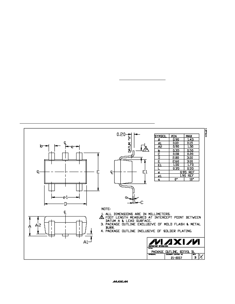
Package Information
Layout Considerations
High switching frequencies make PC board layout a
very important part of design. Good design minimizes
excessive EMI on the feedback paths and voltage gra-
dients in the ground plane, both of which can result in
instability or regulation errors. Connect the inductor,
input filter capacitor, and output filter capacitor as
close to the device as possible, and keep their traces
short, direct, and wide. Connect their ground pins at a
single common node in a star ground configuration.
The external voltage-feedback network should be very
close to the FB pin, within 0.2 inches (5mm). Keep
noisy traces, such as the LX trace, away from the volt-
age-feedback network; also keep them separate, using
grounded copper. The MAX1733/MAX1734 evaluation
kit data sheet includes a proper PC board layout and
routing scheme.
Chip Information
TRANSISTOR COUNT: 1190
PROCESS: BiCMOS
