Absolute maximum ratings, Electrical characteristics – Rainbow Electronics MAX608 User Manual
Page 2
Supply Current
MAX608
5V or Adjustable, Low-Voltage,
Step-Up DC-DC Controller
2
_______________________________________________________________________________________
ABSOLUTE MAXIMUM RATINGS
Supply Voltage
OUT to GND.............................................................-0.3V, 17V
EXT, CS, REF, SHDN, FB to GND ...............-0.3V, (V
OUT
+ 0.3V)
GND to AGND.............................................................0.1V, -0.1V
Continuous Power Dissipation (T
A
= +70°C)
Plastic DIP (derate 9.09mW/°C above +70°C) ............727mW
SO (derate 5.88mW/°C above +70°C) .........................471mW
Operating Temperature Range ...........................-40°C to +85°C
Junction Temperature ......................................................+150°C
Storage Temperature Range .............................-65°C to +160°C
Lead Temperature (soldering, 10sec) .............................+300°C
Stresses beyond those listed under “Absolute Maximum Ratings” may cause permanent damage to the device. These are stress ratings only, and functional
operation of the device at these or any other conditions beyond those indicated in the operational sections of the specifications is not implied. Exposure to
absolute maximum rating conditions for extended periods may affect device reliability.
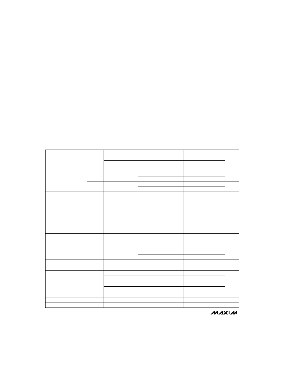
ELECTRICAL CHARACTERISTICS
(V
OUT
= 5V, I
LOAD
= 0mA, T
A
= -40°C to +85°C where indicated. T
A
= -25°C to +85°C for all other limits. Typical values are at
T
A
= +25°C.)
PARAMETER
SYMBOL
CONDITIONS
MIN
TYP
MAX
UNITS
85
110
µ
A
Output Voltage (Note 3)
V
V
IN
= 2.0V to 5.0V,
over full load range,
circuit of Figure 2a
4.825
5.0
5.175
7
mV/V
60
mV/A
Maximum Switch On-Time
t
ON
(max)
12
16
20
µ
s
Minimum Switch Off-Time
t
OFF
(min)
1.8
2.3
2.8
µ
s
%
Reference Voltage
I
REF =
0
µ
A
T
A
= -25°C to +85°C
1.4625
1.5
1.5375
V
T
A
= -40°C to +85°C (Note 1)
1.4475
1.5525
Output Voltage Line
Regulation (Note 4)
Output Voltage Load
Regulation (Note 4)
V
OUT
= 16.5V,
SHDN
≤
0.4V
Minimum Start-Up Voltage
No load
1.6
1.8
V
T
A
= -25°C to +85°C
1.8
16.5
T
A
= -40°C to +85°C (Note 1)
1.9
16.5
Input Voltage Range
(Note 2)
V
Efficiency
87
REF Load Regulation
-4
10
mV
0µA
≤
I
REF
≤
100µA
3V
≤
V
OUT
≤
16.5V
40
100
FB Trip Point Voltage
(Note 5)
V
FB
T
A
= -25°C to +85°C
1.4625
1.5
1.5375
V
T
A
= -40°C to +85°C (Note 1)
1.4475
1.5525
V
OUT
= 1.8V to 16.5V
1.6
µ
V/V
REF Line Regulation
V
IN
= 4V, V
OUT
= 5V, I
LOAD
= 500mA,
circuit of Figure 2a
V
IN
= 2V, V
OUT
= 5V, I
LOAD
= 0mA to 500mA,
circuit of Figure 2a
V
IN
= 2.7V to 4.0V, V
OUT
= 5V, I
LOAD
= 500mA,
circuit of Figure 2a
T
A
= -25°C to +85°C
T
A
= -25°C to +85°C
120
T
A
= -40°C to +85°C (Note 1)
V
OUT
= 10V,
SHDN
≥
1.6V
2
5
µ
A
T
A
= -25°C to +85°C
10
T
A
= -40°C to +85°C (Note 1)
T
A
= -40°C to +85°C (Note 1)
4.800
5.0
5.200
V
REF
V
IH
SHDN Input High Voltage
V
V
IL
SHDN Input Low Voltage
V
V
OUT
= 1.8V to 16.5V
0.4
SHDN Input Current
I
IN
V
OUT
= 16.5V, SHDN = 0V or 16.5V
±1
µ
A
FB Input Current
I
FB
T
A
= -25°C to +85°C
-4
±20
nA
T
A
= -40°C to +85°C (Note 1)
±40