Rainbow Electronics MAX1843 User Manual
Page 2
MAX1843
2.7A, 1MHz, Low-Voltage, Step-Down Regulator with
Internal Synchronous Rectification in QFN Package
2
_______________________________________________________________________________________
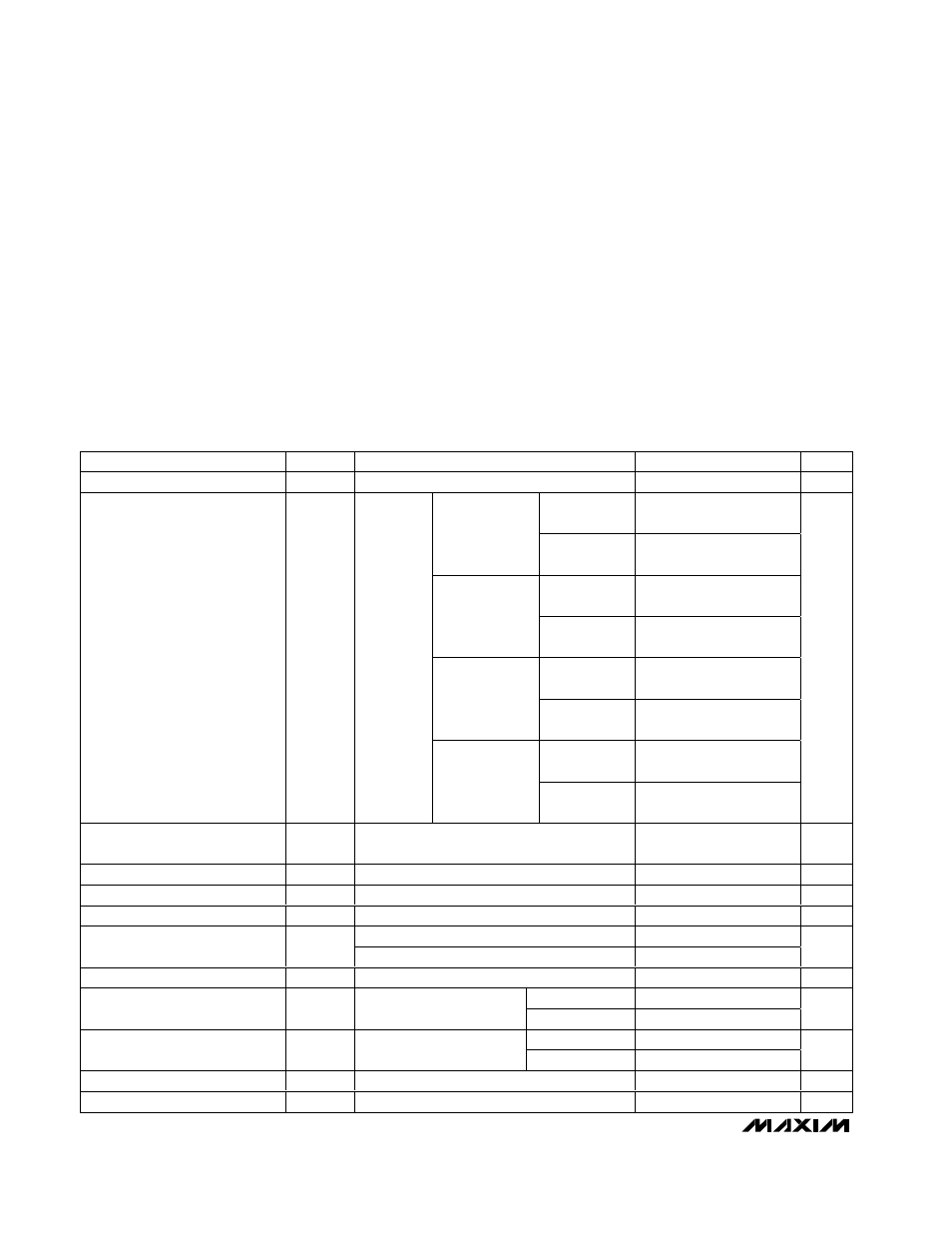
ABSOLUTE MAXIMUM RATINGS
ELECTRICAL CHARACTERISTICS
(V
IN
= V
CC
= +3.3V, FBSEL = GND, T
A
= 0°C to +85°C, unless otherwise noted. Typical values are at T
A
= +25°C.)
Stresses beyond those listed under “Absolute Maximum Ratings” may cause permanent damage to the device. These are stress ratings only, and functional
operation of the device at these or any other conditions beyond those indicated in the operational sections of the specifications is not implied. Exposure to
absolute maximum rating conditions for extended periods may affect device reliability.
V
CC
, IN to GND ........................................................-0.3V to +6V
IN to V
CC
.............................................................................±0.3V
GND to PGND.....................................................................±0.3V
All Other Pins to GND.................................-0.3V to (V
CC
+ 0.3V)
LX Current (Note 1).............................................................±4.7A
REF Short Circuit to GND Duration ............................Continuous
ESD Protection .....................................................................±2kV
Continuous Power Dissipation (T
A
= +70°C)
28-Pin QFN (derate 20mW/°C above +70°C, part mounted
on 1in
2
of 1oz copper)......................................................1.6W
Operating Temperature Range ...........................-40°C to +85°C
Storage Temperature Range .............................-65°C to +150°C
Junction Temperature ......................................................+150°C
Lead Temperature (soldering, 10s) ................................ +300°C
PARAMETER
SYMBOL
CONDITIONS
MIN
TYP
MAX
UNITS
Input Voltage
V
IN
, V
CC
3.0
5.5
V
T
A
= +25°C
to +85°C
2.500
2.525
2.550
FBSEL = V
CC
T
A
= 0°C to
+85°C
2.487
2.525
2.563
T
A
= +25°C
to +85°C
1.500
1.515
1.530
FBSEL =
unconnected
T
A
= 0°C to
+85°C
1.492
1.515
1.538
T
A
= +25°C
to +85°C
1.800
1.818
1.836
FBSEL = REF
T
A
= 0°C to
+85°C
1.791
1.818
1.845
T
A
= +25°C
to +85°C
1.089
1.100
1.111
Preset Output Voltage
V
OUT
V
IN
=
+3V to
+5.5V
I
LOAD
=
0 to 2.5A
V
FB
=
V
OUT
FBSEL = GND
T
A
= 0°C to
+85°C
1.084
1.100
1.117
V
Adjustable Output Voltage
Range
V
IN
= V
CC
= +3V to +5.5V, FBSEL = GND
V
REF
V
IN
V
AC Load Regulation Error
2
%
DC Load Regulation Error
0.4
%
Dropout Voltage
V
DO
V
IN
= V
CC
= +3V, I
LOAD
= 1A
250
mV
T
A
= +25°C to +85°C
1.089
1.100
1.111
Reference Voltage
V
REF
T
A
= 0°C to +85°C
1.084
1.100
1.117
V
Reference Load Regulation
∆V
REF
I
REF
= -1µA to +10µA
0.5
2
mV
V
IN
= +4.5V
90
200
PMOS Switch On-Resistance
R
ON,P
I
LX
= 0.5A
V
IN
= +3V
110
250
m
Ω
V
IN
= +4.5V
70
150
NMOS Switch On-Resistance
R
ON,N
I
LX
= 0.5A
V
IN
= +3V
80
200
m
Ω
Current-Limit Threshold
I
LIMIT
3.1
3.6
4.1
A
RMS LX Output Current
3.1
A
Note 1: LX has internal clamp diodes to PGND and IN. Applications that forward bias these diodes should take care not to exceed the
IC’s package power dissipation limits.