Chip information – Rainbow Electronics MAX1843 User Manual
Page 11
MAX1843
2.7A, 1MHz, Low-Voltage, Step-Down Regulator with
Internal Synchronous Rectification in QFN Package
______________________________________________________________________________________
11
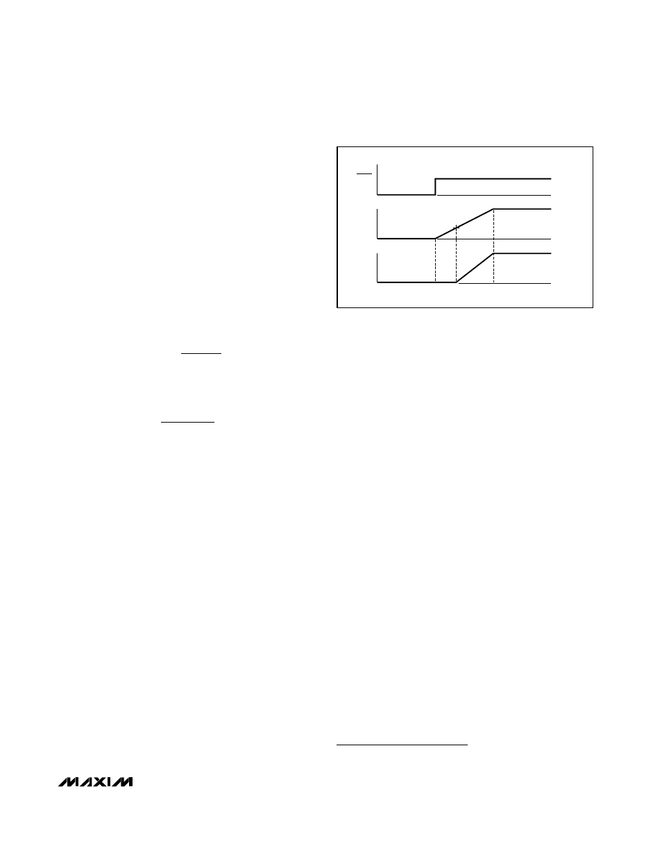
Soft-Start
Soft-start allows a gradual increase of the internal cur-
rent limit to reduce input surge currents at startup and
at exit from shutdown. A timing capacitor, C
SS
, placed
from SS to GND sets the rate at which the internal cur-
rent limit is changed. Upon power-up, when the device
comes out of undervoltage lockout (2.6V typ) or after
the SHDN pin is pulled high, a 4µA constant-current
source charges the soft-start capacitor and the voltage
on SS increases. When the voltage on SS is less than
approximately 0.7V, the current limit is set to zero. As
the voltage increases from 0.7V to approximately 1.8V,
the current limit is adjusted from 0 to the current-limit
threshold (see the Electrical Characteristics). The volt-
age across the soft-start capacitor changes with time
according to the equation:
The soft-start current limit varies with the voltage on the
soft-start pin, SS, according to the equation:
where I
LIMIT
is the current threshold from the Electrical
Characteristics.
The constant-current source stops charging once the
voltage across the soft-start capacitor reaches 1.8V
(Figure 5).
Frequency Variation with Output Current
The operating frequency of the MAX1843 is determined
primarily by t
OFF
(set by R
TOFF
), V
IN
, and V
OUT
as
shown in the following formula:
f
PWM
= (V
IN
- V
OUT
- V
PMOS
) / [t
OFF
(V
IN
- V
PMOS
+
V
NMOS
)]
However, as the output current increases, the voltage
drop across the NMOS and PMOS switches increases
and the voltage across the inductor decreases. This
causes the frequency to drop. The change in frequency
can be approximated with the following formula:
∆f
PWM
= -I
OUT
x R
PMOS
/ (V
IN
x t
OFF
)
where R
PMOS
is the resistance of the internal MOSFETs
(90m
Ω typ).
Circuit Layout and Grounding
Good layout is necessary to achieve the MAX1843’s
intended output power level, high efficiency, and low
noise. Good layout includes the use of ground planes,
careful component placement, and correct routing of
traces using appropriate trace widths. The following
points are in order of decreasing importance:
1) Minimize switched-current and high-current ground
loops. Connect the input capacitor’s ground, the out-
put capacitor’s ground, and PGND. Connect the
resulting island to GND at only one point.
2) Connect the input filter capacitor less than 5mm
away from IN. The connecting copper trace carries
large currents and must be at least 1mm wide,
preferably 2.5mm.
3) Place the LX node components as close together
and as near to the device as possible. This reduces
resistive and switching losses as well as noise.
4) Ground planes are essential for optimum perfor-
mance. In most applications, the circuit is located on
a multilayer board and full use of the four or more
layers is recommended. For heat dissipation, con-
nect the exposed backside pad to a large analog
ground plane, preferably on a surface of the board
that receives good airflow. If the ground plane is
located on the IC surface, make use of the N.C. pins
adjacent to GND to lower thermal resistance to the
ground plane. If the ground is located elsewhere,
use several vias to lower thermal resistance. Typical
applications use multiple ground planes to minimize
thermal resistance. Avoid large AC currents through
the analog ground plane.
Chip Information
TRANSISTOR COUNT: 3662
SSI
V
V
V
I
LIMIT
SS
LIMIT
=
×
−
.
.
0 7
1 1
V
A
t
C
SS
SS
=
×
4
µ
0.7V
1.8V
I
LIMIT
t
SHDN
0
0
0
V
SS
(V)
I
LIMIT
(A)
Figure 5. Soft-Start Current-Limit Over Time