Definitions – Rainbow Electronics MAX1230 User Manual
Page 19

MAX1226/MAX1228/MAX1230
12-Bit 300ksps ADCs with FIFO,
Temp Sensor, Internal Reference
______________________________________________________________________________________
19
CS
DOUT
SCLK
DIN
EOC
MSB1
LSB1
MSB2
(ACQUISITION1)
(ACQUISITION2)
(CONVERSION1)
(CONVERSION BYTE)
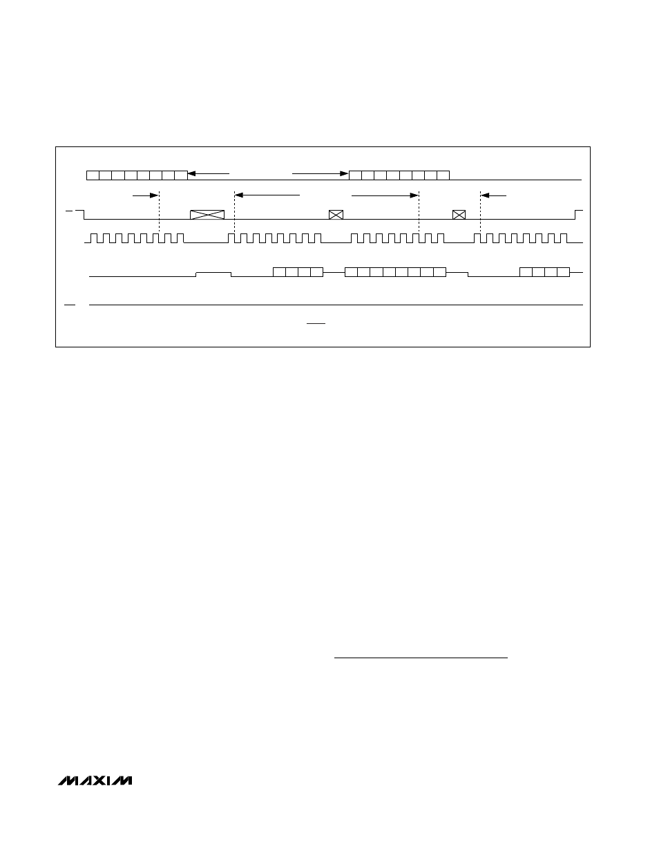
EXTERNALLY TIMED ACQUISITION, SAMPLING AND CONVERSION WITHOUT CNVST.
Figure 7. Clock Mode 11
Initiate a conversion by writing a byte to the conversion
register followed by 16 SCLK cycles. If CS is pulsed
high between the eighth and ninth cycles, the pulse
width must be less than 100µs. To continuously con-
vert at 16 cycles per conversion, alternate 1 byte of
zeros between each conversion byte.
If reference mode 00 is requested, or if an external ref-
erence is selected but a temperature measurement is
being requested, wait 65µs with CS high after writing
the conversion byte to extend the acquisition and allow
the internal reference to power up. To perform a tem-
perature measurement, write 24 bytes (192 cycles) of
zeros after the conversion byte. The temperature result
appears on DOUT during the last 2 bytes of the
192 cycles.
Partial Reads and Partial Writes
If the first byte of an entry in the FIFO is partially read
(CS is pulled high after fewer than eight SCLK cycles),
the second byte of data that is read out contains the
next 8 bits (not b7–b0). The remaining bits are lost for
that entry. If the first byte of an entry in the FIFO is read
out fully, but the second byte is read out partially, the
rest of the entry is lost. The remaining data in the FIFO
is uncorrupted and can be read out normally after tak-
ing CS low again, as long as the 4 leading bits (nor-
mally zeros) are ignored. Internal registers that are
written partially through the SPI contain new values,
starting at the MSB up to the point that the partial write
is stopped. The part of the register that is not written
contains previously written values. If CS is pulled low
before EOC goes low, a conversion cannot be com-
pleted and the FIFO is corrupted.
Transfer Function
Figure 8 shows the unipolar transfer function for single-
ended or differential inputs.
Figure 9
shows the bipolar
transfer function for differential inputs. Code transitions
occur halfway between successive-integer LSB values.
Output coding is binary, with 1 LSB = V
REF
/ 4096V for
unipolar and bipolar operation, and 1 LSB = 0.125°C
for temperature measurements.
Layout, Grounding, and Bypassing
For best performance, use PC boards. Do not use wire-
wrap boards. Board layout should ensure that digital
and analog signal lines are separated from each other.
Do not run analog and digital (especially clock) signals
parallel to one another or run digital lines underneath the
MAX1226/MAX1228/MAX1230 package. High-frequen-
cy noise in the V
DD
power supply can affect perfor-
mance. Bypass the V
DD
supply with a 0.1µF capacitor
to GND, close to the V
DD
pin. Minimize capacitor lead
lengths for best supply-noise rejection. If the power sup-
ply is very noisy, connect a 10
Ω resistor in series with
the supply to improve power-supply filtering. For the
QFN package, connect its exposed pad to ground.
Definitions
Integral Nonlinearity
Integral nonlinearity (INL) is the deviation of the values
on an actual transfer function from a straight line. This
straight line can be either a best-straight-line fit or a
line drawn between the end points of the transfer func-
tion, once offset and gain errors have been nullified.
INL for the MAX1226/MAX1228/MAX1230 is measured
using the end-point method.
