Rainbow Electronics MAX1230 User Manual
Page 15
MAX1226/MAX1228/MAX1230
12-Bit 300ksps ADCs with FIFO,
Temp Sensor, Internal Reference
______________________________________________________________________________________
15
Reset Register
Write to the reset register (as shown in Table 7) to clear
the FIFO or to reset all registers to their default states.
Set the RESET bit to 1 to reset the FIFO. Set the reset
bit to zero to return the MAX1226/MAX1228/MAX1230
to its default power-up state.
Power-Up Default State
The MAX1226/MAX1228/MAX1230 power up with all
blocks in shutdown, including the reference. All registers
power up in state 00000000, except for the setup regis-
ter, which powers up in clock mode 10 (CKSEL1 = 1).
Temperature Measurements
The MAX1226/MAX1228/MAX1230 perform tempera-
ture measurements with an internal diode-connected
transistor. The diode bias current changes from 68µA
to 4µA to produce a temperature-dependent bias volt-
age difference. The second conversion result at 4µA is
subtracted from the first at 68µA to calculate a digital
value that is proportional to absolute temperature. The
output data appearing at DOUT is the above digital
code minus an offset to adjust from Kelvin to Celsius.
The reference voltage used for the temperature mea-
surements is derived from the internal reference source
to ensure a resolution of 1/8 of a degree.
Output Data Format
Figures 4–7 illustrate the conversion timing for the
MAX1226/MAX1228/MAX1230. The 12-bit conversion
result is output in MSB-first format with 4 leading zeros.
DIN data is latched into the serial interface on the rising
edge of SCLK. Data on DOUT transitions on the falling
edge of SCLK. Conversions in clock modes 00 and 01
are initiated by CNVST. Conversions in clock modes 10
and 11 are initiated by writing an input data byte to the
conversion register. Data is binary for unipolar mode and
two’s complement for bipolar mode.
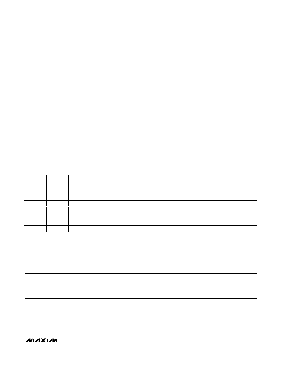
BIT NAME
BIT
FUNCTION
UCH0/1
7 (MSB)
Set to 1 to configure AIN0 and AIN1 for unipolar differential conversion.
UCH2/3
6
Set to 1 to configure AIN2 and AIN3 for unipolar differential conversion.
UCH4/5
5
Set to 1 to configure AIN4 and AIN5 for unipolar differential conversion.
UCH6/7
4
Set to 1 to configure AIN6 and AIN7 for unipolar differential conversion.
UCH8/9
3
Set to 1 to configure AIN8 and AIN9 for unipolar differential conversion (MAX1228/MAX1230 only).
UCH10/11
2
Set to 1 to configure AIN10 and AIN11 for unipolar differential conversion (MAX1228/MAX1230 only).
UCH12/13
1
Set to 1 to configure AIN12 and AIN13 for unipolar differential conversion (MAX1230 only).
UCH14/15
0 (LSB)
Set to 1 to configure AIN14 and AIN15 for unipolar differential conversion (MAX1230 only).
Table 4. Unipolar Mode Register (Addressed Through Setup Register)
BIT NAME
BIT
FUNCTION
BCH0/1
7 (MSB)
Set to 1 to configure AIN0 and AIN1 for bipolar differential conversion.
BCH2/3
6
Set to 1 to configure AIN2 and AIN3 for bipolar differential conversion.
BCH4/5
5
Set to 1 to configure AIN4 and AIN5 for bipolar differential conversion.
BCH6/7
4
Set to 1 to configure AIN6 and AIN7 for bipolar differential conversion.
BCH8/9
3
Set to 1 to configure AIN8 and AIN9 for bipolar differential conversion (MAX1228/MAX1230 only).
BCH10/11
2
Set to 1 to configure AIN10 and AIN11 for bipolar differential conversion (MAX1228/MAX1230 only).
BCH12/13
1
Set to 1 to configure AIN12 and AIN13 for bipolar differential conversion (MAX1230 only).
BCH14/15
0 (LSB)
Set to 1 to configure AIN14 and AIN15 for bipolar differential conversion (MAX1230 only).
Table 5. Bipolar Mode Register (Addressed Through Setup Register)