Design procedure, Table 2. output voltage control – Rainbow Electronics MAX1672 User Manual
Page 8

MAX1672
Step-Up/Down DC-DC Converter
in QSOP Package
8
_______________________________________________________________________________________
__________________Design Procedure
Output Voltage Selection
For fixed output voltages of 3.3V or 5V, connect 3/5 to
PS or GND and connect FB to GND (Table 2).
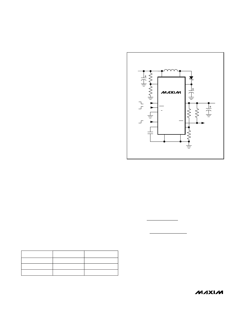
Alternatively, adjust the output voltage from 1.25V to
5.5V by connecting two resistors, R1 and R2 (Figure 2),
which form a voltage divider between OUT and FB.
Choose resistor values as follows:
R1 = R2[(V
OUT
/ V
REF
) -1]
where V
REF
= 1.25V. Since the input bias current at FB
has a maximum value of 50nA, R1 and R2 can be large
with no significant accuracy loss. Choose R2 in the
100k
Ω
to 270k
Ω
range and calculate R1 using the
above formula. For 1% error, the current through R1
should be at least 100 times FB’s bias current.
Whenever the voltage at FB exceeds 70mV above
GND, the state of the 3/5 pin is ignored. Connect 3/5 to
GND when adjusting V
OUT
with a resistor divider. Never
leave 3/5 unconnected.
Low-Battery Detection
The MAX1672 contains a comparator for low-battery
detection. If the voltage at PGI falls below V
REF
(typical-
ly 1.25V), the open-drain comparator output (PGO)
goes high. Hysteresis is typically 30mV. Set the low-
battery detector’s threshold with resistors R3 and R4
(Figure 2) using the following equation:
R3 = R4[(V
PGT
/ V
REF
) -1]
where V
PGT
is the desired threshold of the low-battery
detector and V
REF
= 1.25V. Since the input bias current
at PGI has a maximum value of 50nA, R3 and R4 can
be large to minimize input loading with no significant
accuracy loss. Choose R4 in the 100k
Ω
to 270k
Ω
range
and calculate R3 using the above formula. For 1%
error, the current through R3 should be at least 100
times PGI’s bias current.
The PGO output is open-drain and should be pulled
high with external resistor R5 for normal operation. If the
low-battery comparator is not used, connect PGI and
PGO to GND.
Inductor Selection
A 10µH inductor performs well in most MAX1672 appli-
cations. Smaller inductor values typically offer a smaller
physical size for a given series resistance, but may
increase switching losses. Larger inductor values
exhibit higher output current capability and larger phys-
ical dimensions for a given series resistance. For opti-
mum performance, choose an inductor value from
Table 3 or by using the following equation:
where I
LIM
is the peak switch-current limit, which is
0.8A for I
LIM
= PS and 0.5A for I
LIM
= GND.
The inductor’s incremental saturation current rating
should also be greater than the peak switch-current
limit. However, it is generally acceptable to bias most
inductors into saturation by as much as 20% with slight-
ly reduced efficiency. The inductor’s DC resistance sig-
nificantly affects efficiency. See Tables 4 and 5 for a list
of suggested inductors and suppliers.
V
+ V
I
V
+ V
I
OUT
DIODE
LIM
IN(min)
SWITCH
LIM
(
)
<
<
(
)
t
L
t
OFF
ON
2
(max)
MAX1672
IN
ONA
PGI
ONB
OFF
ON
C3
0.1
µ
F
C1
100
µ
F
C2
100
µ
F
R2
R1
R5
1M
C4
4.7
µ
F
R3
R4
L1
10
µ
H
PGND
GND
PS
1.25V TO
5.5V OUTPUT
INPUT
1.8V TO 11V
LOW-BATTERY-
DETECTOR
OUTPUT
OUT
PG0
FB
REF
LX
OFF
3/5
ILIM
0.8A
ON
0.5A
Figure 2. Adjustable Output Voltage Configuration
Table 2. Output Voltage Control
FB
V
OUT
(V)
0
GND
+5
1
GND
+3.3
3/
5
5
X
>70mV
+1.25 to +5.5
