Pin description, Typical operating characteristics (continued) – Rainbow Electronics MAX1672 User Manual
Page 5

MAX1672
Step-Up/Down DC-DC Converter
in QSOP Package
_______________________________________________________________________________________
5
______________________________________________________________Pin Description
NAME
FUNCTION
1
LX
Inductor Connection to the Drain of the Internal N-Channel Power MOSFET
PIN
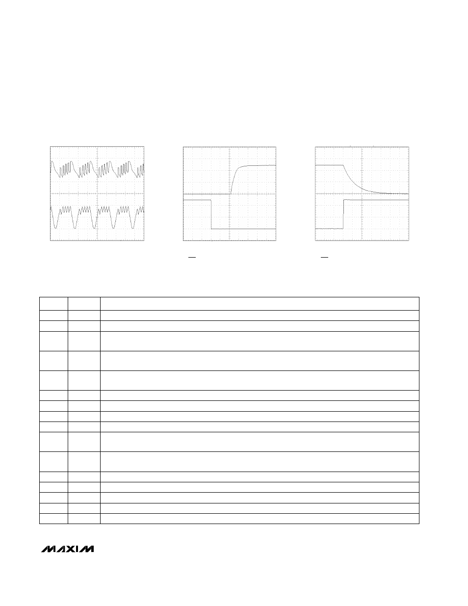
_____________________________Typical Operating Characteristics (continued)
(T
A
= +25°C, unless otherwise noted.)
A
B
10
µ
s/div
OUTPUT RIPPLE (HEAVY LOAD)
MAX1672-13
A: V
OUT
= 5V (20mV/div, AC COUPLED)
B: I
L1
(500mA /div) (V
IN
= 2.7V, I
OUT
= 250mA)
A
B
50
µ
s/div
START-UP DELAY
MAX1672-14
A: V
OUT
= (2V/div)
B: ONB (2V/div) (V
IN
= 2.7V, R
LOAD
= 50
Ω
)
A
B
200
µ
s/div
TURN-OFF DELAY
MAX1672-15
A: V
OUT
= (2V/div)
B: ONB (2V/div) (V
IN
= 2.7V, R
LOAD
= 50
Ω
)
2
PGND
Power Ground
3
ONB
On Control Input. When ONB = low or ONA = high, the IC is on. Connect ONB to GND for normal operation
(Table 1).
4
ONA
On Control Input. When ONA = low and ONB = high, the IC is off. Connect ONA to PS for normal operation
(Table 1).
5
3/5
Output Voltage Selection Input. Connect to PS for 3.3V output and to GND for 5V output. With V
FB
> 80mV,
the state of the 3/5 pin is ignored. (Table 2).
6
PGI
Low-Battery Detector Input (1.25V threshold)
7
PGO
Low-Battery Detector Output (open drain). PGO pulls low when V
PGI
is greater than 1.25V.
8
ILIM
Inductor-Current-Limit Selection Input. Connect to PS for 0.8A current limit and to GND for 0.5A current limit.
9
OUT
Regulator Output. Drain of internal PFET linear regulator. Bypass with a 4.7µF capacitor to GND.
10
FB
Feedback Input. For 3.3V or 5V output, connect to GND. For adjustable output, connect to feedback resistor-
divider network. With V
FB
> 70mV, the state of the 3/5 pin is ignored.
11
PS
Bootstrapped Power Supply. Output of step-up switch-mode regulator and source of internal PFET linear
regulator. The IC is powered from this pin.
12
IN
Input Voltage Sense Input. Connect to input supply.
13
REF
Reference Voltage Output. Bypass with a 0.1µF capacitor to GND.
14
GND
Analog Ground
15
PGND
Power Ground
16
LX
Inductor Connection to the Drain of the Internal N-Channel Power MOSFET
