Detailed description, Pin description – Rainbow Electronics MAX1524 User Manual
Page 5
Detailed Description
The MAX1522/MAX1523/MAX1524 are simple, com-
pact boost controllers designed for a wide range of
DC-DC conversion topologies including step-up,
SEPIC, and flyback applications. These devices are
designed specifically to provide a simple application
circuit with a minimum of external components and are
ideal for PDAs, digital cameras, and other low-cost
consumer electronics applications.
These devices use a unique fixed on-time, minimum
off-time architecture, which provides excellent efficien-
cy over a wide range of input/output voltage combina-
tions and load currents. The fixed on-time is pin
selectable to either 0.5µs or 3µs, permitting optimiza-
tion of external component size and ease of design for
a wide range of output voltages.
Control Scheme
The MAX1522/MAX1523/MAX1524 feature a unique
fixed on-time, minimum off-time architecture, which pro-
vides excellent efficiency over a wide range of
input/output voltage combinations. The fixed on-time is
pin selectable to either 0.5µs or 3µs for a maximum
duty factor of either 45% or 80%, respectively. An
inductor charging cycle is initiated by driving EXT high,
turning on the external MOSFET. The MOSFET remains
on for the fixed on-time, after which EXT turns off the
MOSFET. EXT stays low for at least the minimum off-
time, and another cycle begins when FB drops below
its 1.25V regulation point.
Bootstrapped vs. Nonbootstrapped
The V
CC
supply voltage range of the MAX1522/
MAX1523/MAX1524 is +2.5V to +5.5V. The supply for
V
CC
can come from the input voltage (nonboot-
strapped), the output voltage (bootstrapped), or an
independent regulator.
The MAX1522/MAX1523 are usually utilized in a non-
bootstrapped configuration, allowing for high or low
output voltage operation. However, when both the input
and output voltages fall within the +2.5V to +5.5V
range, the MAX1522/MAX1523 may be operated in
nonbootstrapped or bootstrapped mode. Bootstrapped
mode provides higher gate-drive voltage to the MOS-
FET switch, reducing I
2
R losses in the switch, but will
also increase the V
CC
supply current to charge and
discharge the gate. Depending upon the MOSFET
selected, there may be minor variation in efficiency vs.
load vs. input voltage when comparing bootstrapped
and nonbootstrapped configurations.
The MAX1524 is always utilized in bootstrapped config-
uration for applications where the input voltage range
extends down below 2.5V and the output voltage is
between 2.5V and 5.5V. V
CC
is connected to the output
(through a 10
Ω
series resistor) and receives startup
voltage through the DC current path from the input
through the inductor, diode, and 10
Ω
resistor. The
MAX1524 features a low-voltage startup oscillator that
MAX1522/MAX1523/MAX1524
Simple SOT23 Boost Controllers
_______________________________________________________________________________________
5
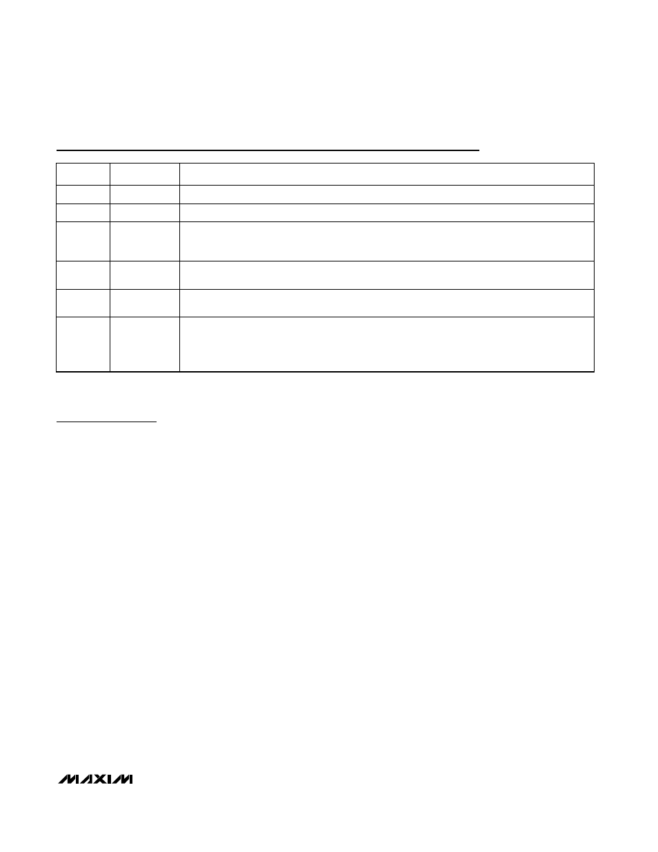
Pin Description
PIN
NAME
FUNCTION
1
GND
Ground
2
FB
Feedback Input. Connect FB to external resistive voltage-divider. FB regulates to 1.25V.
3
SET
On-Time Control. Connect SET to V
CC
to set the fixed 3
µ
s on-time (85% duty cycle). Connect SET to
GND to set the fixed 0.5
µ
s on-time (50% duty cycle). See On-Time SET Input section for more
information.
4
SHDN
Shutdown Control Input. Drive SHDN high for normal operation. Drive SHDN low for low-power
shutdown mode. Driving SHDN low clears the fault latch of the MAX1522 and MAX1524.
5
EXT
External MOSFET Drive. EXT drives the gate of an external NMOS power FET and swings from V
CC
to GND.
6
V
CC
Supply Voltage to the IC. Bypass V
CC
to GND with a 0.1
µ
F capacitor. Connect V
CC
to a +2.5V to
+5.5V supply, which may come from V
IN
(nonbootstrapped) or V
OUT
(bootstrapped) or from the
output of another regulator. For bootstrapped operation, connect V
CC
to the output through a series
10
Ω
resistor.