Table 14. r, Modulator, Output noise – Rainbow Electronics MAX1402 User Manual
Page 26
MAX1402
+5V, 18-Bit, Low-Power, Multichannel,
Oversampling (Sigma-Delta) ADC
26
______________________________________________________________________________________
ensuring that REFIN+ is more positive than REFIN-.
REFIN+ and REFIN- must be between AGND and V+.
The MAX1402 is specified with a +2.5V reference when
operating with a +5V analog supply (V+).
Modulator
The MAX1402 performs analog-to-digital conversion
using a single-bit, second-order, switched-capacitor
modulator. A single comparator within the modulator
quantizes the input signal at a much higher sample rate
than the bandwidth of the signal to be converted. The
quantizer then presents a stream of 1s and 0s to the
digital filter for processing, to remove the frequency-
shaped quantization noise.
The MAX1402 modulator provides 2nd-order frequency
shaping of the quantization noise resulting from the sin-
gle bit quantizer. The modulator is fully differential for
maximum signal-to-noise ratio and minimum suscepti-
bility to power-supply noise.
The modulator operates at one of a total of eight differ-
ent sampling rates (f
M
) determined by the master clock
frequency (f
CLKIN
), the X2CLK bit, the CLK bit, and the
modulator frequency control bits MF1 and MF0. Power
dissipation is optimized for each of these modes by
controlling the bias level of the modulator. Table 15
shows the input and reference sample rates.
PGA
A programmable gain amplifier (PGA) with a user-
selectable gain of x1, x2, x4, x8, x16, x32, x64, or x128
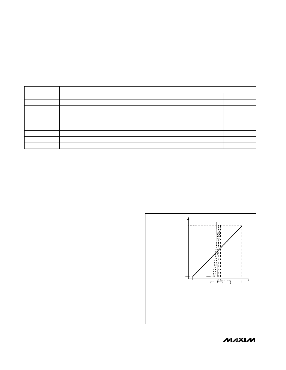
(Table 6) precedes the modulator. Figure 7 shows the
default bipolar transfer function with the following illus-
trated codes: 1) PGA = 0, DAC = 0; 2) PGA = 3, DAC =
0; or 3) PGA = 3, DAC = 3.
Output Noise
Tables 16a and 16b show the rms noise for typical out-
put frequencies (notches) and -3dB frequencies for the
MAX1402 with f
CLKIN
= 2.4576MHz. The numbers
given are for the bipolar input ranges with V
REF
=
+2.50V, with no buffer (BUFF = 0) and with the buffer
inserted (BUFF = 1). These numbers are typical and
are generated at a differential analog input voltage of 0.
Figure 8 shows graphs of Effective Resolution vs. Gain
and Notch Frequency. The effective resolution values
were derived from the following equation:
Table 14. R
EXT
, C
EXT
Values for Less than 16-Bit Gain Error in Buffered (BUFF = 1)
Mode—All Modulator Sampling Frequencies (MF1, MF0 = XX); X2CLK = 0; CLKIN =
2.4576MHz
10
10
10
10
10
2
10
10
10
10
4
1
C
EXT
= 0pF
C
EXT
= 50pF
C
EXT
= 100pF
10
10
10
10
10
10
10
10
PGA GAIN
10
C
EXT
= 500pF
C
EXT
= 1000pF
C
EXT
= 5000pF
EXTERNAL RESISTANCE R
EXT
(k
Ω
)
10
10
10
10
10
16
10
10
10
10
32
8
10
10
10
10
10
10
10
10
10
10
10
10
64
10
10
10
128
10
10
10
10
10
10
ZERO-SCALE 2621
MIDSCALE 131072
NEGATIVE DAC STEP
SHIFTS THE TRANSFER
FUNCTION TOWARD
THE POSITIVE RAIL.
PGA = 3
DAC = 0
PGA = 0
DAC = 0
PGA = 3
DAC = +3
MAX CODE 262144
FULL-SCALE 259522
INPUT VOLTAGE RANGE
CODE
(V
AIN
-)-V
REF
AGND
(V
AIN
-) - V
REF
/8 - V
REF
/16
(V
AIN
-) - V
REF
/8 - V
REF
/16
(V
AIN
-) - V
REF
/8
(V
AIN
-) + V
REF
/8
V+
(V
AIN
-) + V
REF
(V
AIN-
)
Figure 7. Effect of PGA and DAC Codes on the Bipolar
Transfer Function