Max1730, Detailed description, Functional diagram – Rainbow Electronics MAX1730 User Manual
Page 6

MAX1730
Detailed Description
The MAX1730 step-down charge pump automatically
switches between charge pump configurations (Figures
1, 2, and 3) and utilizes pulse-skipping pulse-frequency
modulation (PFM) to provide a regulated output voltage
with high efficiency. The output voltage is pin-selectable
to 1.8V or 1.9V. The MAX1730 accepts inputs between
2.7V and 5.5V and guarantees up to 50mA output cur-
rent.
Charge-Pump Configurations
Charge pumps work by passing energy through capaci-
tors. They generally work in two phases. In the first phase,
the input source charges the flying capacitors. The input
capacitor helps reduce the source’s input impedance. In
the second phase, the switching capacitors transfer their
charge to the output as needed.
Figure 1 shows the 1:1 charge-pump configuration. C1
and C2 charge in parallel between IN and GND during
the first phase. In the second phase, C1 and C2 connect
in parallel between OUT and GND.
Figure 2 shows the 3:2 charge-pump configuration. C1
and C2 charge in parallel between IN and OUT during
the first phase. In the second phase, C1 and C2 connect
in series between OUT and GND.
Figure 3 shows the 2:1 charge-pump configuration. C1
and C2 charge in parallel between IN and OUT during
the first phase. In the second phase, C1 and C2 connect
in parallel between OUT and GND.
Pulse-Skipping PFM and Mode
Transitions
In the MAX1730, pulse-skipping PFM mode pauses the
oscillator when the output is in regulation. Using the 2:1
charge-pump configuration as an example, when the
output is set to half the input, the switching frequency is
near the oscillator frequency. However, for outputs below
half the input, switching pauses once the desired output
level is achieved. With no output current, the device
switches occasionally. With higher levels of current, the
switching frequency increases to supply the load.
50mA Regulated Step-Down Charge Pump
for 1.8V or 1.9V Logic
6
_______________________________________________________________________________________
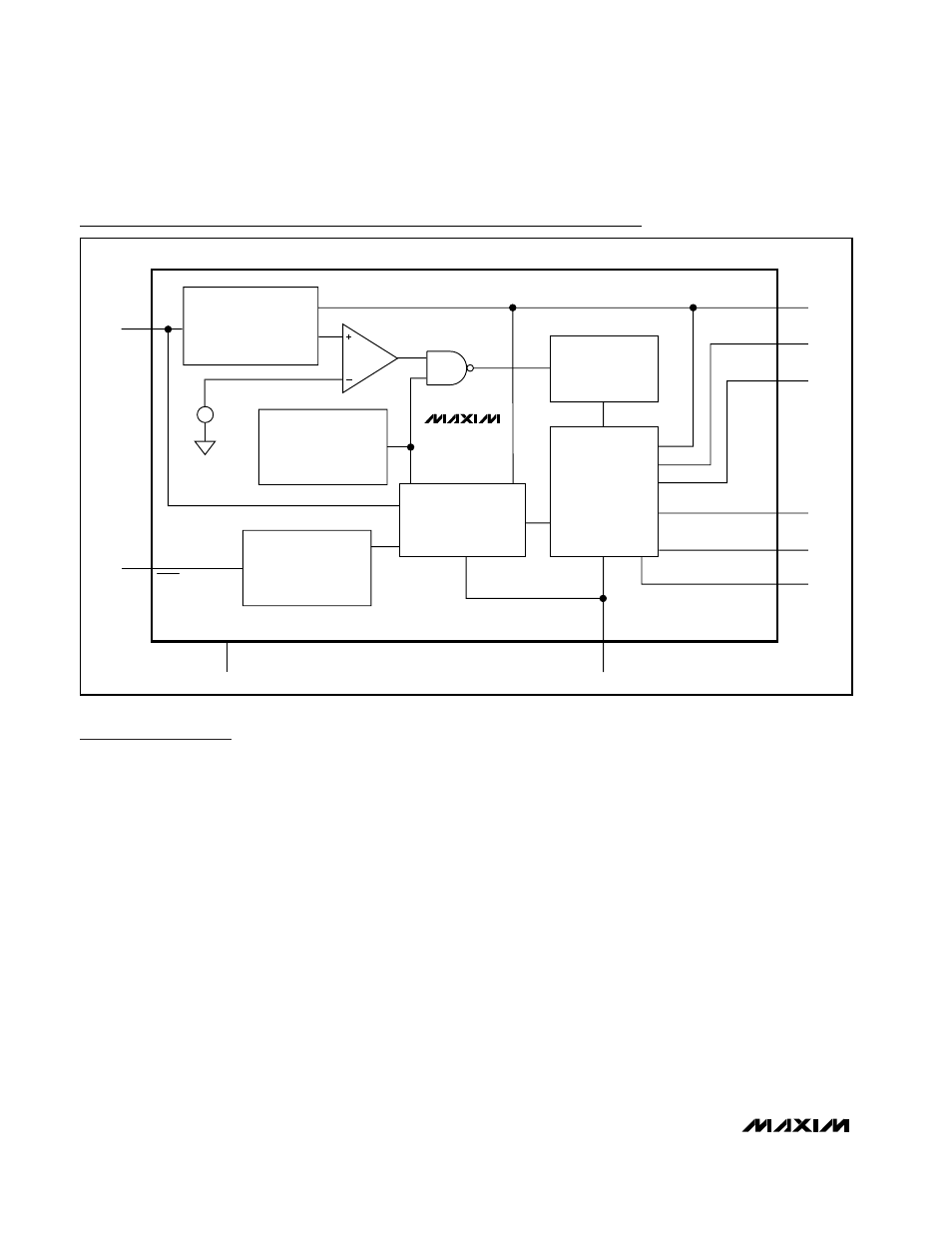
Functional Diagram
FB CONTROL
OSCILLATOR
SHUTDOWN
SHDN
GND
FB
VREF
+
CONTROL LOGIC
MAX1730
IN
PGND
C2N
C2P
C1N
C1P
OUT
SWITCH ARRAY
DRIVERS
