Inverting dc-dc controllers, Design procedure – Rainbow Electronics MAX776 User Manual
Page 11

using bootstrapped or non-bootstrapped mode will
directly affect the gate drive to the FET. EXT swings
from V+ to V
OUT
. In bootstrapped operation, OUT is
connected to the output voltage (-5V, -12V, -15V). In
non-bootstrapped operation, OUT is connected to
ground, and EXT now swings from V+ to ground.
At high input-to-output differentials, it may be neces-
sary to use non-bootstrapped mode to avoid the 21V
V+ to V
OUT
maximum rating. Also, observe the V
GS
maximum rating of the external transistor. At intermedi-
ate voltages and currents, the advantages of boot-
strapped vs. non-bootstrapped operation are slight.
When input voltages are less than about 4V, always use
the bootstrapped circuit.
Shutdown and Quiescent Current
The MAX774/MAX775/MAX776 are designed to save
power in battery-powered applications. A TTL/CMOS
logic-level shutdown input (SHDN) has been provided
for the lowest-power applications. When shut down
(SHDN = V+), most internal bias current sources and
the reference are turned off so that less than 5µA of
current is drawn.
In normal operation, the quiescent current will be less
than 100µA. However, this current is measured by
forcing the external switch transistor off. Even with no
load, in an actual application, additional current will be
drawn to supply the feedback resistors’ and the diode’s
and capacitor’s leakage current. Under no-load condi-
tions, you should see a short current pulse at half the
peak current approximately every 100ms (the exact
period depends on actual circuit leakages).
EXT Drive Voltages
EXT swings from OUT to V+ and provides the drive out-
put for an external power MOSFET. When using the on-
chip feedback resistors for the preset output voltages,
the voltage at OUT equals the output voltage. When
using external feedback resistors, OUT may be tied to
GND or some other potential between V
OUT
and GND.
Always observe the V+ to OUT absolute maximum rat-
ing of 21V. For V+ to output differentials greater than
21V, OUT must be tied to a potential more positive than
the output and, therefore, the output voltage must be
set with an external resistor divider.
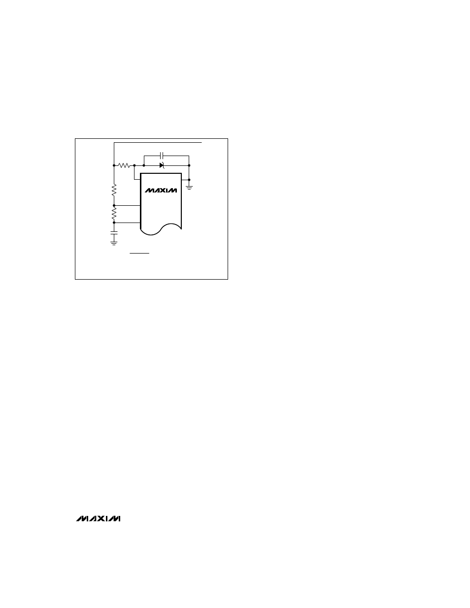
In non-bootstrapped operation with low input voltages
(<4V), tie OUT to a negative voltage to fully enhance the
external MOSFET. Accomplish this by creating an inter-
mediate voltage for V
OUT
with a zener diode (Figure 5).
__________________Design Procedure
Setting the Output Voltage
The MAX774/MAX775/MAX776 are preset for -5V, -12V,
and -15V output voltages, respectively; however, they
may also be adjusted to other values with an external
voltage divider. For the preset output voltage, connect
FB to REF and connect OUT to the output (Figure 3). In
this case, the output voltage is sensed by OUT.
For an adjustable output (Figures 3 and 4), connect an
external resistor divider from the output voltage to FB,
and from FB to REF. In this case, the divided-down
output voltage is sensed via the FB pin.
There are three reasons to use the external resistor divider:
1) You desire an output voltage other than a preset
value
2) The input-to-output differential exceeds 21V
or
3) The output voltage (V
OUT
to GND) exceeds -15V.
For adjustable operation, refer to Figures 3 and 4. The
impedance of the feedback network should be low
enough that the input bias current of FB is not a factor.
For best efficiency and precision, allow 10µA to flow
through the network. Calculate (V
REF
- V
FB
) / R1 =
10µA. Since V
REF
= 1.5V and V
FB
= 0V, R1 becomes
150k
Ω
. Then calculate R2 as follows:
R2
V
OUT
___ = _______
R1
V
REF
(or, V
OUT
= 10
µ
A)
______
R2
MAX774/MAX775/MAX776
-5V/-12V/-15V or Adjustable,
High-Efficiency, Low I
Q
Inverting DC-DC Controllers
______________________________________________________________________________________
11
Figure 5. Connection Using Zener Diode to Boost Base Drive
R1
MAX774
MAX775
MAX776
OUT
GND
FB
R2
8
2
1
REF
4
0.1
µ
F
0.1
µ
F
V
OUT
R
Z
6V
≤
V
Z
+ V
IN
≤
10V
VOUT
– V
Z
> I
Z
R
Z
I
Z
= ZENER BREAKDOWN CURRENT
V
Z
= ZENER BREAKDOWN VOLTAGE
V
IN
= INPUT SUPPLY VOLTAGE
