Max619 regulated 5v charge-pump dc-dc converter, Chip topography – Rainbow Electronics MAX619 User Manual
Page 7

MAX619
Regulated 5V Charge-Pump
DC-DC Converter
________________________________________________________________________________________
7
Layout Considerations
The MAX619’s high oscillator frequency makes good
layout important. A good layout ensures stability and
helps maintain the output voltage under heavy loads.
For best performance, use very short connections to
the capacitors.
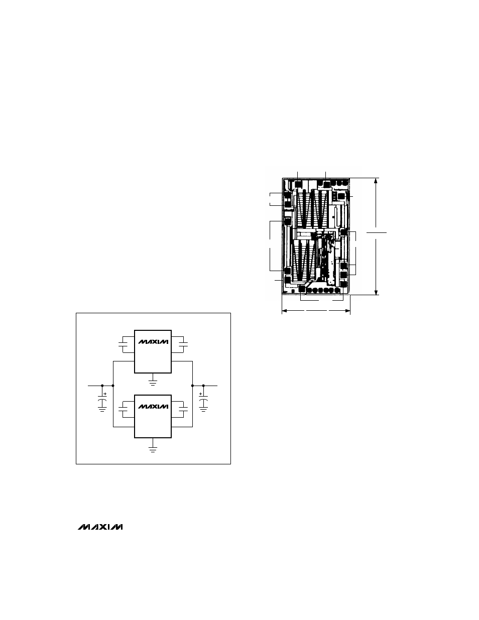
Paralleling Devices
Two MAX619s can be placed in parallel to increase
output drive capability. The IN, OUT, and GND pins
can be paralleled, but C1 and C2 pins cannot. The
input bypass capacitor and output filter capacitor are,
to some extent, shared when two circuits are paral-
leled. If the circuits are physically close together, it
may be possible to use a single bypass and a single
output capacitor, each with twice the value of the single
circuit. If the MAX619s cannot be placed close togeth-
er, use separate bypass and output capacitors. The
amount of output ripple observed will determine
whether single input bypass and output filter capacitors
can be used.
___________________Chip Topography
C1+
C1-
SHDN
GND
0.115”
(2.921mm)
IN
OUT
C2+
C2-
0.072”
(1.828mm)
TRANSISTOR COUNT: 599;
SUBSTRATE CONNECTED TO GND.
MAX619
IN
OUT
GND
INPUT
5V, 40mA
MAX619
IN
OUT
GND
Figure 3. Paralleling Two MAX619s
