Rainbow Electronics AT89S52 User Manual
Features, Description, Pin configurations
1
Features
•
Compatible with MCS-51
™
Products
•
8K Bytes of In-System Reprogrammable Flash Memory
•
Endurance: 1,000 Write/Erase Cycles
•
Fully Static Operation: 0 Hz to 24 MHz
•
Three-level Program Memory Lock
•
256 x 8-bit Internal RAM
•
32 Programmable I/O Lines
•
Three 16-bit Timer/Counters
•
Eight Interrupt Sources
•
Programmable Serial Channel
•
Low-power Idle and Power-down Modes
Description
The AT89C52 is a low-power, high-performance CMOS 8-bit microcomputer with 8K
bytes of Flash programmable and erasable read only memory (PEROM). The device
is manufactured using Atmel’s high-density nonvolatile memory technology and is
compatible with the industry-standard 80C51 and 80C52 instruction set and pinout.
The on-chip Flash allows the program memory to be reprogrammed in-system or by a
conventional nonvolatile memory programmer. By combining a versatile 8-bit CPU
with Flash on a monolithic chip, the Atmel AT89C52 is a powerful microcomputer
which provides a highly-flexible and cost-effective solution to many embedded control
applications.
8-bit
Microcontroller
with 8K Bytes
Flash
AT89C52
Rev. 0313H–02/00
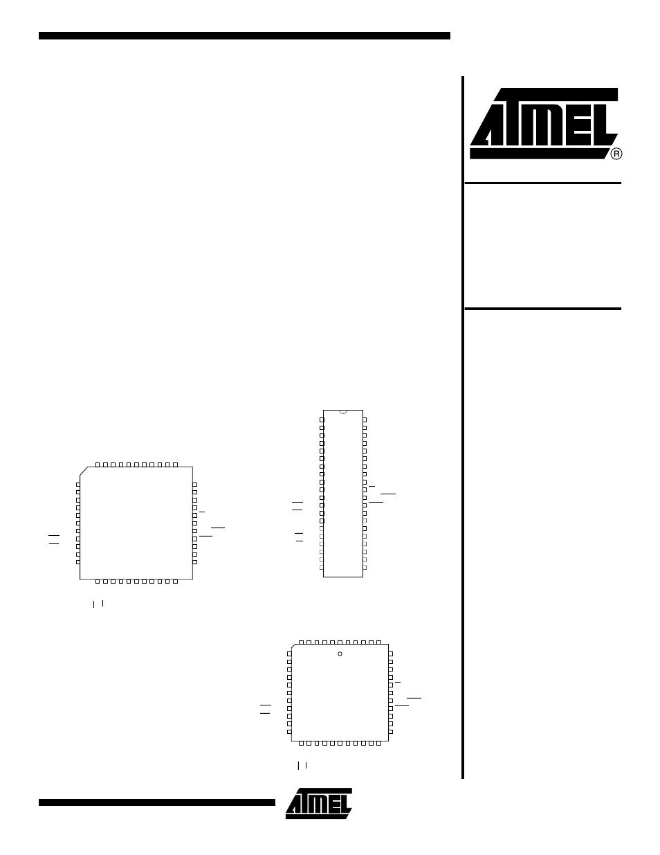
Pin Configurations
PQFP/TQFP
1
2
3
4
5
6
7
8
9
10
11
33
32
31
30
29
28
27
26
25
24
23
P1.5
P1.6
P1.7
RST
(RXD) P3.0
NC
(TXD) P3.1
(INT0) P3.2
(INT1) P3.3
(T0) P3.4
iT1) P3.5
P0.4 (AD4)
P0.5 (AD5)
P0.6 (AD6)
P0.7 (AD7)
EA/VPP
NC
ALE/PROG
PSEN
P2.7 (A15)
P2.6 (A14)
P2.5 (A13)
44
43
42
41
40
39
38
37
36
35
34
12
13
14
15
16
17
18
19
20
21
22
(WR) P3.6
(RD) P3.7
XTAL2
XTAL1
GND
NC
(A8) P2.0
(A9) P2.1
(A10) P2.2
(A11) P2.3
(A12) P2.4
P1.4
P1.3
P1.2
P1.1 (T2 EX)
P1.0 (T2)
NC
VCC
P0.0 (AD0)
P0.1 (AD1)
P0.2 (AD2)
P0.3 (AD3)
PDIP
1
2
3
4
5
6
7
8
9
10
11
12
13
14
15
16
17
18
19
20
40
39
38
37
36
35
34
33
32
31
30
29
28
27
26
25
24
23
22
21
(T2) P1.0
(T2 EX) P1.1
P1.2
P1.3
P1.4
P1.5
P1.6
P1.7
RST
(RXD) P3.0
(TXD) P3.1
(INT0) P3.2
(INT1) P3.3
(T0) P3.4
(T1) P3.5
(WR) P3.6
(RD) P3.7
XTAL2
XTAL1
GND
VCC
P0.0 (AD0)
P0.1 (AD1)
P0.2 (AD2)
P0.3 (AD3)
P0.4 (AD4)
P0.5 (AD5)
P0.6 (AD6)
P0.7 (AD7)
EA/VPP
ALE/PROG
PSEN
P2.7 (A15)
P2.6 (A14)
P2.5 (A13)
P2.4 (A12)
P2.3 (A11)
P2.2 (A10)
P2.1 (A9)
P2.0 (A8)
PLCC
7
8
9
10
11
12
13
14
15
16
17
39
38
37
36
35
34
33
32
31
30
29
P1.5
P1.6
P1.7
RST
(RXD) P3.0
NC
(TXD) P3.1
(INT0) P3.2
(INT1) P3.3
(T0) P3.4
(T1) P3.5
P0.4 (AD4)
P0.5 (AD5)
P0.6 (AD6)
P0.7 (AD7)
EA/VPP
NC
ALE/PROG
PSEN
P2.7 (A15)
P2.6 (A14)
P2.5 (A13)
6
5
4
3
2
1
44
43
42
41
40
18
19
20
21
22
23
24
25
26
27
28
(WR) P3.6
(RD) P3.7
XTAL 2
XTAL1
GND
NC
(A8) P2.0
(A9) P2.1
(A10) P2.2
(A11) P2.3
(A12) P2.4
P1.4
P1.3
P1.2
P1.1 (T2 EX)
P1.0 (T2)
NC
VCC
P0.0 (AD0)
P0.1 (AD1)
P0.2 (AD2)
P0.3 (AD3)
Document Outline
- Pin Configurations
- Features
- Description
- Block Diagram
- Pin Description
- Special Function Registers
- Data Memory
- Timer 0 and 1
- Timer 2
- Baud Rate Generator
- Programmable Clock Out
- UART
- Interrupts
- Oscillator Characteristics
- Idle Mode
- Power-down Mode
- Status of External Pins During Idle and Powe-down Modes
- Program Memory Lock Bits
- Lock Bit Protection Modes
- Programming the Flash
- Programming Interface
- Flash Programming Modes
- Flash Programming and Verification Characteristics
- Flash Programming and Verification Waveforms - High-voltage Mode (VPP=12V)
- Flash Programming and Verification Waveforms - Low-voltage Mode (VPP=5V)
- Absolute Maximum Ratings*
- DC Characteristics
- AC Characteristics
- External Program and Data Memory Characteristics
- External Program Memory Read Cycle
- External Data Memory Read Cycle
- External Data Memory Write Cycle
- External Clock Drive Waveforms
- External Clock Drive
- Serial Port Timing: Shift Register Mode Test Conditions
- Shift Register Mode Timing Waveforms
- AC Testing Input/Output Waveforms(1)
- Float Waveforms(1)
- Ordering Information