Figure 5. differential drive circuit of, Table 3. resistor values for circuit of, 3 input common mode voltage – Rainbow Electronics ADC12D040 User Manual
Page 19: 0 digital inputs, 1 clk, Figure 5, Table 3. resistor values for circuit of ns4771, Applications information
Applications Information
(Continued)
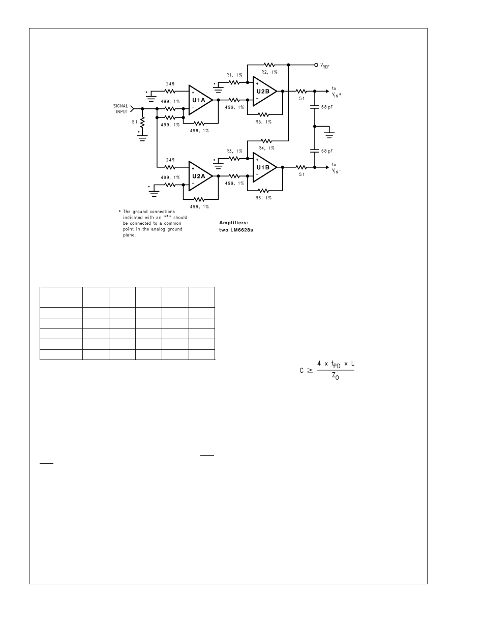
TABLE 3. Resistor Values for Circuit of Figure 5
SIGNAL
RANGE
R1
R2
R3
R4
R5, R6
0 - 0.25V
140
Ω
768
Ω
226
Ω
412
Ω 2000Ω
0 - 0.5V
255
Ω
768
Ω
976
Ω
698
Ω 1000Ω
0 - 1.0V
464
Ω
768
Ω
976
Ω
137
Ω
499
Ω
±
0.25V
845
Ω
499
Ω
845
Ω
499
Ω 2000Ω
±
0.5V
845
Ω
499
Ω
845
Ω
499
Ω
499
Ω
1.3.3 Input Common Mode Voltage
The input common mode voltage, V
CM
, should be of a value
such that the peak excursions of the analog signal does not
go more negative than ground or more positive than 1.0
Volts below the V
A
supply voltage. The nominal V
CM
should
generally be about V
REF
/2. V
RM
A and V
RM
B can be used as
V
CM
sources as long as no d.c. current is drawn from these
pins.
2.0 DIGITAL INPUTS
Digital TTL/CMOS compatible inputs consist of CLK, OEA,
OEB and PD.
2.1 CLK
The CLK signal controls the timing of the sampling process.
Drive the clock input with a stable, low jitter clock signal in
the range of 100 kHz to 55 MHz with rise and fall times of
less than 3ns. The trace carrying the clock signal should be
as short as possible and should not cross any other signal
line, analog or digital, not even at 90˚.
If the CLK is interrupted, or its frequency too low, the charge
on internal capacitors can dissipate to the point where the
accuracy of the output data will degrade. This is what limits
the lowest sample rate to 100 kSPS.
The ADC clock line should be considered to be a transmis-
sion line and be series terminated at the source end to match
the source impedance with the characteristic impedance of
the clock line. It generally is not necessary to terminate the
far (ADC) end of the clock line, but if a single clock source is
driving more than one device (a condition that is generally
not recommended), far end termination may be needed. Far
end termination is a series RC with the resistor being the
same as the characteristic impedance of the clock line. The
capacitor should have a minimum value of
20046060
where t
PD
is the propagation time in ns/unit length, "L" is the
length of the line and Z
O
is the characteristic impedance of
the line. The units of t
PD
and "L" should be consistent with
each other. The typical board of FR-4 material has a t
PD
of
about 150 ps/inch, or about 60 ps/cm.
The far end termination should be near but beyond the ADC
clock pin as seen from the clock source.
The duty cycle of the clock signal can affect the performance
of any A/D Converter. Because achieving a precise duty
cycle is difficult, the ADC12040 is designed to maintain
performance over a range of duty cycles. While it is specified
and performance is guaranteed with a 50% clock duty cycle,
performance is typically maintained over a clock duty cycle
range of 40% to 60%.
Take care to maintain a constant clock line impedance
throughout the length of the line. Refer to Application Note
AN-905 for information on setting characteristic impedance.
20046014
FIGURE 5. Differential Drive Circuit of Figure 4
ADC12D040
www.national.com
19