Pin descriptions and equivalent circuits – Rainbow Electronics ADC12L066 User Manual
Page 3
Pin Descriptions and Equivalent Circuits
Pin No.
Symbol
Equivalent Circuit
Description
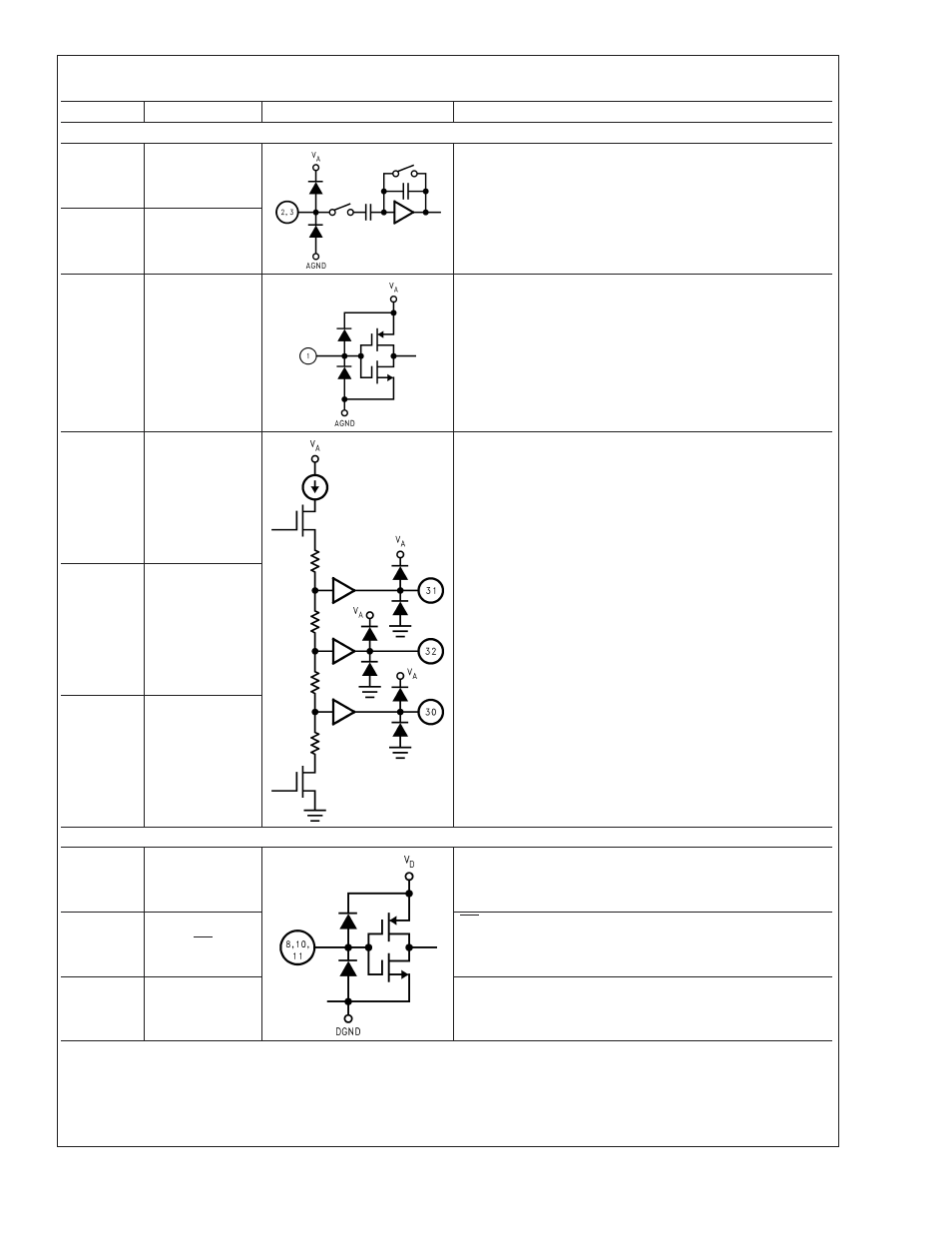
ANALOG I/O
2
V
IN+
Analog signal Input pins. With a 1.0V reference voltage the
differential input signal level is 2.0 V
P-P
. The V
IN
- pin may be
connected to V
CM
for single-ended operation, but a differential
input signal is required for best performance.
3
V
IN−
1
V
REF
Reference input. This pin should be bypassed to AGND with
a 0.1 µF monolithic capacitor. V
REF
is 1.0V nominal and
should be between 0.8V and 1.5V.
31
V
RP
These pins are high impedance reference bypass pins.
Connect a 0.1 µF capacitor from each of these pins to AGND.
DO NOT LOAD these pins.
32
V
RM
30
V
RN
DIGITAL I/O
10
CLK
Digital clock input. The range of frequencies for this input is
1 MHz to 80 MHz (typical) with guaranteed performance at 66
MHz. The input is sampled on the rising edge of this input.
11
OE
OE is the output enable pin that, when low, enables the
TRI-STATE
®
data output pins. When this pin is high, the
outputs are in a high impedance state.
8
PD
PD is the Power Down input pin. When high, this input puts
the converter into the power down mode. When this pin is
low, the converter is in the active mode.
ADC12L066
www.national.com
3