Instruction set, Flash parallel programming modes, At89s53 – Rainbow Electronics AT89S53 User Manual
Page 21
AT89S53
21
.
Notes:
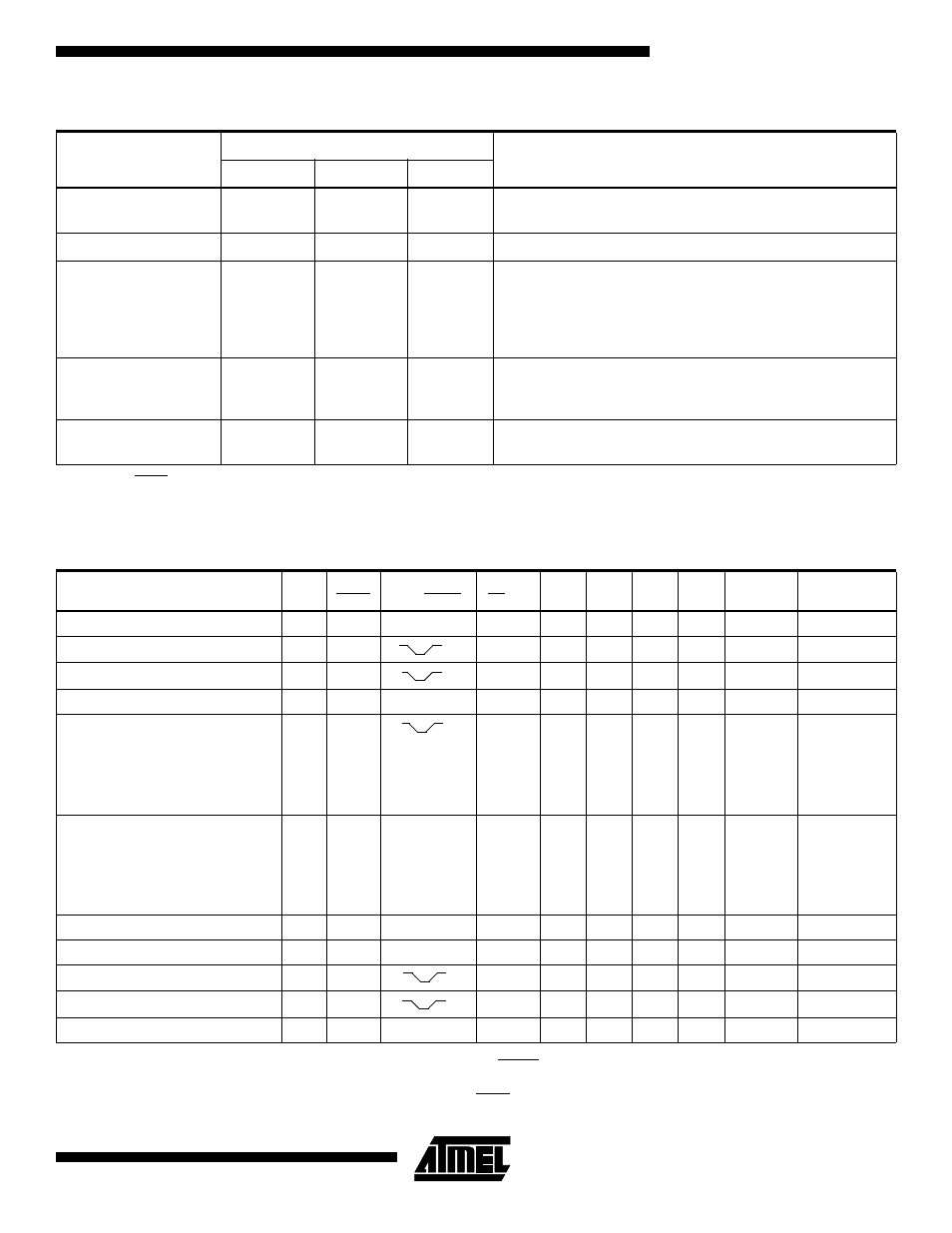
1. “h” = weakly pulled “High” internally.
2. Chip Erase and Serial Programming Fuse require a 10 ms PROG pulse. Chip Erase needs to be performed first before
reprogramming any byte with a content other than FFH.
3. P3.4 is pulled Low during programming to indicate RDY/BSY.
4. “X” = don’t care
Flash Parallel Programming Modes
Mode
RST
PSEN
ALE/PROG
EA/V
PP
P2.6
P2.7
P3.6
P3.7
Data I/O
P0.7:0
Address
P2.5:0 P1.7:0
Serial Prog. Modes
H
h
h
x
Chip Erase
H
L
12V
H
L
L
L
X
X
Write (12K bytes) Memory
H
L
12V
L
H
H
H
DIN
ADDR
Read (12K bytes) Memory
H
L
H
12V
L
L
H
H
DOUT
ADDR
Write Lock Bits:
H
L
12V
H
L
H
L
DIN
X
Bit - 1
P0.7 = 0
X
Bit - 2
P0.6 = 0
X
Bit - 3
P0.5 = 0
X
Read Lock Bits:
H
L
H
12V
H
H
L
L
DOUT
X
Bit - 1
@P0.2
X
Bit - 2
@P0.1
X
Bit - 3
@P0.0
X
Read Atmel Code
H
L
H
12V
L
L
L
L
DOUT
30H
Read Device Code
H
L
H
12V
L
L
L
L
DOUT
31H
Serial Prog. Enable
H
L
12V
L
H
L
H
P0.0 = 0
X
Serial Prog. Disable
H
L
12V
L
H
L
H
P0.0 = 1
X
Read Serial Prog. Fuse
H
L
H
12V
H
H
L
H
@P0.0
X
(2)
(2)
(2)
Instruction Set
Notes:
1. DATA polling is used to indicate the end of a write cycle which typically takes less than 10 ms at 2.7V.
2. “x” = don’t care.
Instruction
Input Format
Operation
Byte 1
Byte 2
Byte 3
Programming Enable
1010 1100
0101 0011
xxxx xxxx
Enable serial programming interface after RST goes
high.
Chip Erase
1010 1100
xxxx x100
xxxx xxxx
Chip erase the 12K memory array.
Read Code Memory
low addr
xxxx xxxx
Read data from Code memory array at the selected
address. The 6 MSBs of the first byte are the high order
address bits. The low order address bits are in the
second byte. Data are available at pin MISO during the
third byte.
Write Code Memory
low addr
data in
Write data to Code memory location at selected
address. The address bits are the 6 MSBs of the first
byte together with the second byte.
Write Lock Bits
1010 1100
xxxx xxxx
Write lock bits.
Set LB1, LB2 or LB3 = “0” to program lock bits.
A1
2
A1
1
A1
0
A9
A8
A1
3
01
A12 A11
A10
A9
A8
A13
10
LB1 LB2
LB3
x x111