Pin descriptions and equivalent circuits – Rainbow Electronics ADC10080 User Manual
Page 4

Pin Descriptions and Equivalent Circuits
(Continued)
Pin No.
Symbol
Equivalent Circuit
Description
16–20,
23–27
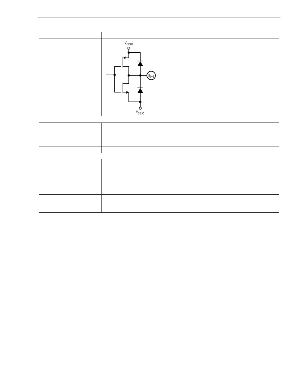
D0–D9
Digital output data. D0 is the LSB and D9 is the MSB of the
binary output word.
ANALOG POWER
2, 9, 10
V
DDA
Positive analog supply pins. These pins should be connected
to a quiet 3.0V source and bypassed to analog ground with a
0.1 µF monolithic capacitor located within 1 cm of these pins.
A 4.7 µF capacitor should also be used in parallel.
3, 11, 14
V
SSA
Ground return for the analog supply.
DIGITAL POWER
22
V
DDIO
Positive digital supply pins for the ADC10080’s output drivers.
This pin should be bypassed to digital ground with a 0.1 µF
monolithic capacitor located within 1 cm of this pin. A 4.7 µF
capacitor should also be used in parallel. The voltage on this
pin should never exceed the voltage on V
DDA
by more than
300 mV.
21
V
SSIO
The ground return for the digital supply for the output drivers.
This pin should be connected to the digital ground, but not
near the analog ground.
ADC10080
www.national.com
4
