Absolute maximum ratings, Dc electrical characteristics, Ac electrical characteristics – Rainbow Electronics DS75LX User Manual
Page 2
DS75LX: Digital Thermometer and Thermostat with Extended Addressing
2
of
13
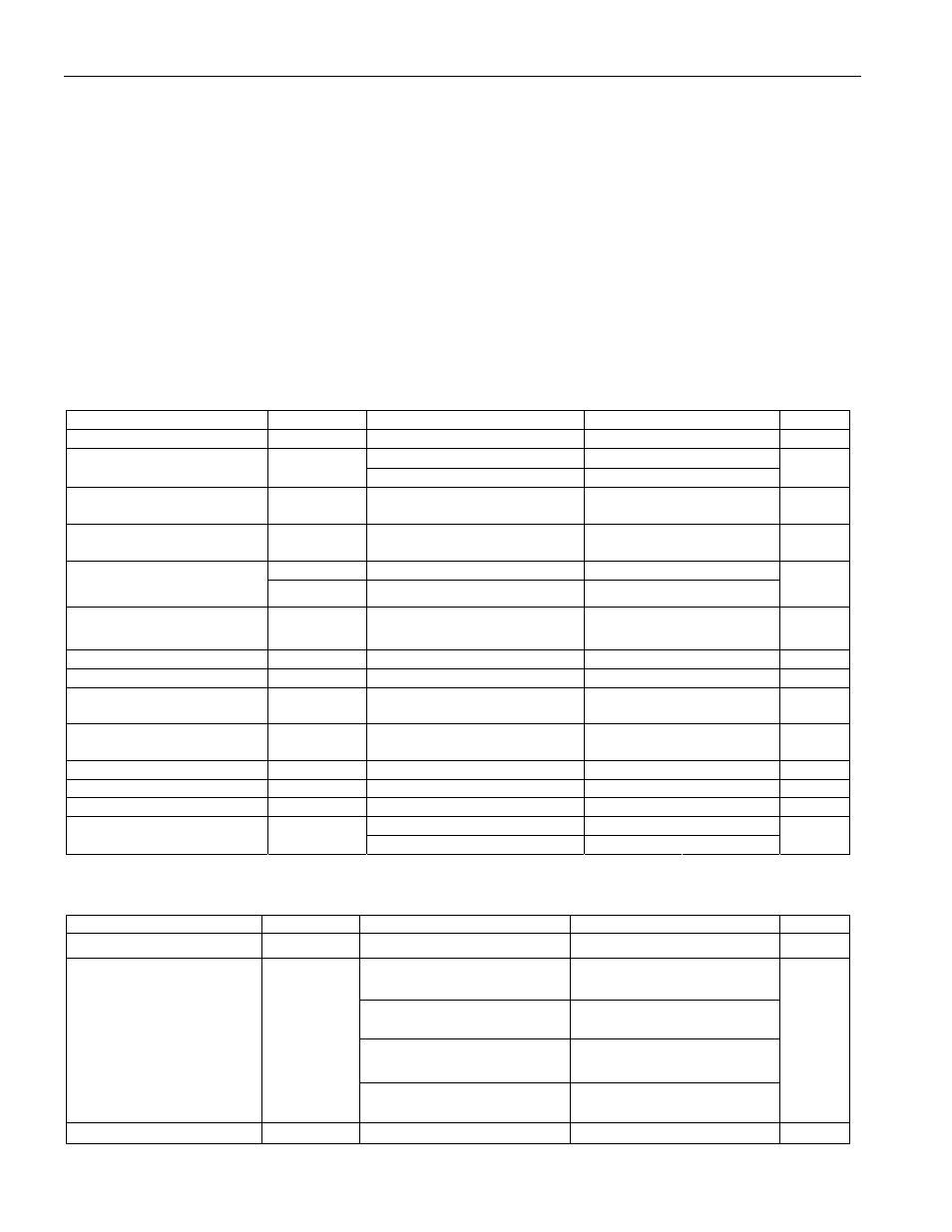
ABSOLUTE MAXIMUM RATINGS
Voltage Range on V
DD
, Relative to Ground
-0.3V to +4.0V
Voltage Range on Any Other Pin, Relative to Ground
-0.3V to +6.0V
Operating
Temperature
Range
-55°C
to
+125°C
Storage
Temperature
Range
-55°C
to
+125°C
Soldering
Temperature
See
IPC/JEDEC
J-STD-020
These are stress ratings only and functional operation of the device at these or any other conditions above those indicated in the operation
sections of this specification is not implied. Exposure to absolute maximum rating conditions for extended periods of time may affect reliability.
The Dallas Semiconductor DS75LX is built to the highest quality standards and manufactured for long-term
reliability. All Dallas Semiconductor devices are made using the same quality materials and manufacturing
methods. However, the DS75LX is not exposed to environmental stresses, such as burn-in, that some industrial
applications require. For specific reliability information on this product, contact the factory in Dallas at (972) 371-
4448.
DC ELECTRICAL CHARACTERISTICS
(1.7V
≤ V
DD
≤ 3.7V, T
A
= -55°C to +125°C.)
PARAMETER SYMBOL CONDITIONS
MIN MAX
UNITS
Supply Voltage
V
DD
(Note
1)
1.7
3.7
V
-25°C to +100°C
±2.0
Thermometer Error
(Note 2)
T
ERR
-55°C to +125°C
±3.0
°C
Input Logic-High SDA,
SCL
V
IH
(Note 3)
0.7 x V
DD
V
DD
+ 0.3
V
Input Logic-Low SDA,
SCL
V
IL
V
SS
- 0.3
0.3 x V
DD
V
V
OL1
3mA sink current
0
0.4
SDA Output Logic-Low
Voltage (Note 3)
V
OL2
6mA sink current
0
0.6
V
O.S. Saturation Voltage
V
OL
4mA sink current
(Notes 2, 3)
0.8
V
Input Current SDA, SCL
0.4 < V
I/O
< 0.9V
DD
-10
+10
µA
I/O Capacitance
C
I/O
10
pF
Address Input Sink
Current
I
LAH
A0, A1, or A2 tied to V
DD
(Notes 4, 5)
0.2 3.5
µA
Address Input Source
Current
I
LAL
A0, A1, or A2 tied to GND
(Notes 4, 5)
0.2 3.5
µA
Address Voltage High
V
AH
(Note
6)
V
DD
- .04
V
Address Voltage Low
V
AL
(Note
6)
V
SS
+ .04
V
Standby Current
I
DD1
(Notes 4, 5)
13
µA
Active temp conversions
1000
Active Current
(Notes 1, 4, 5)
I
DD
Communication only
100
µA
AC ELECTRICAL CHARACTERISTICS
(1.7V
≤ V
DD
≤ 3.7V, T
A
= -55°C to +125°C.)
PARAMETER SYMBOL CONDITIONS MIN
TYP
MAX
UNITS
Resolution
9 12
Bits
9-bit conversions
25
10-bit conversions
50
11-bit conversions
100
Temperature Conversion
Time
t
CONVT
12-bit conversions
200
ms
SCL Frequency
f
SCL
400 kHz