Figure 8. 2-wire interface timing – Rainbow Electronics DS75LX User Manual
Page 13
DS75LX: Digital Thermometer and Thermostat with Extended Addressing
13
of
13
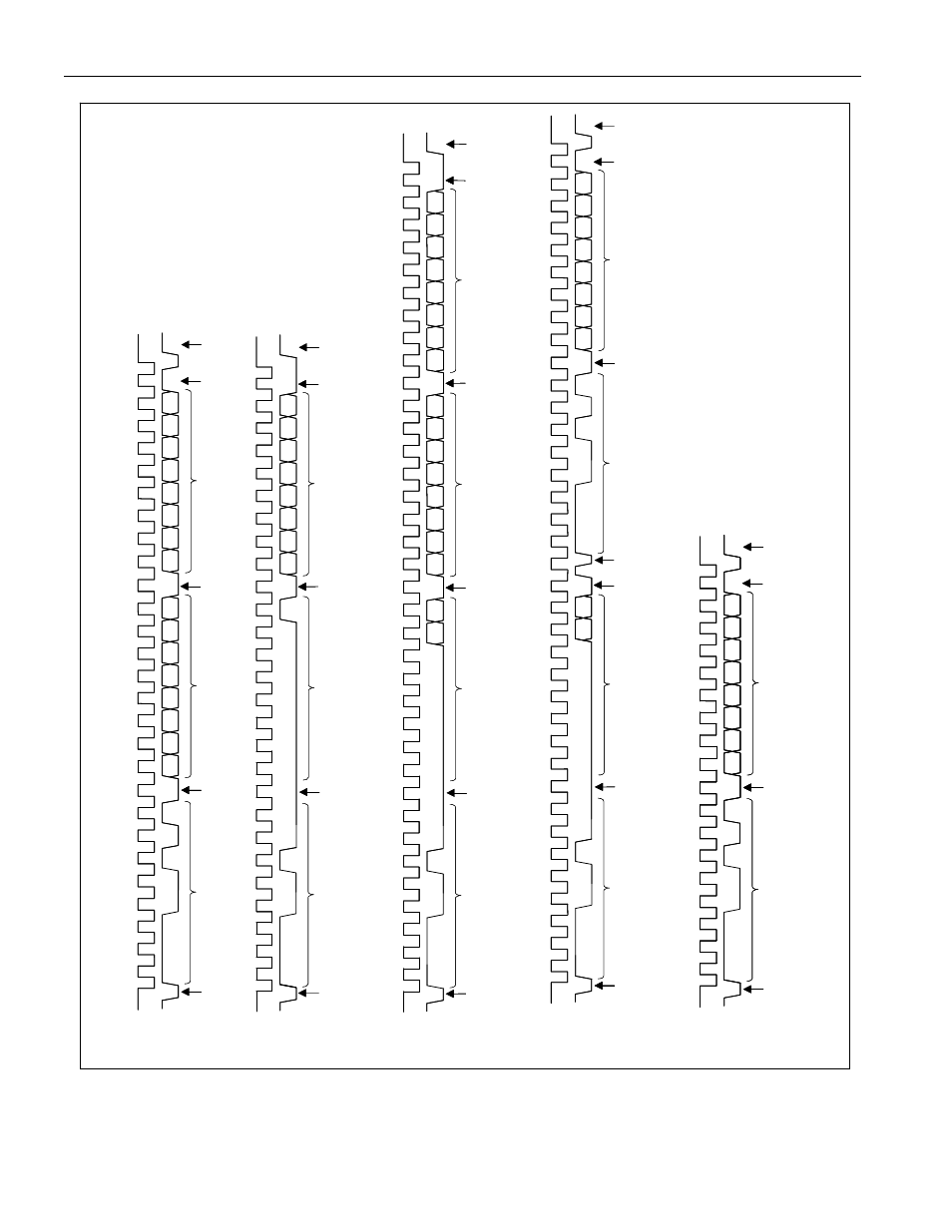
Figure 8. 2-Wire Interface Timing
(DS
7
5
L
X)
(DS7
5LX
)
A
D2
D6
D5
D
4
D3
D1
D0
WA
0
00
0
0
00
1A
D
7
Address Byte
STAR
T
SCL
SDA
ACK
Poi
n
te
r Byt
e
P
Da
ta
B
y
te
(from
Ma
ste
r)
STO
P
ACK
ACK
(DS
7
5
L
X)
A
D2
D6
D5
D
4
D3
D1
D0
WA
0
00
0
0
00
1
0
00
0
0
00
1A
D
7
b) Write to the
Co
nfiguration Register
S
Address Byte
STAR
T
SCL
SDA
ACK
Poi
n
te
r Byt
e
P
Da
ta
B
y
te
(from
Ma
ste
r)
STO
P
ACK
ACK
c)
W
rite
to
t
h
e T
OS
or T
HY
ST
Reg
ist
er
SCL
SDA
W
A
Add
ress Byt
e
STA
R
T
ACK
(D
S75
L
X
)
A
0
0
00
0
0
P1
P0
P
o
in
te
r By
te
ACK
(DS7
5L
X)
D4
D6
D5
D3
D2
D0
D7
D
6
D5
D4
D3
D2
D
1
D0
D7
A
D1
P
LS
Da
ta
By
te
(f
ro
m
M
a
ste
r)
A
MS Da
ta
B
y
te
(fro
m M
a
ster)
STO
P
ACK
(DS
7
5
L
X)
ACK
(DS7
5L
X)
c)
W
rite
to
t
h
e T
OS
or T
HY
ST
Reg
ist
er
SCL
SDA
S
W
A
Add
ress Byt
e
STA
R
T
ACK
A
0
0
00
0
0
P1
P0
0
0
00
0
0
P1
P0
P
o
in
te
r By
te
ACK
D4
D6
D5
D3
D2
D0
D7
D
6
D5
D4
D3
D2
D
1
D0
D7
A
D1
P
LS
Da
ta
By
te
(f
ro
m
M
a
ste
r)
A
MS Da
ta
B
y
te
(fro
m M
a
ster)
STO
P
ACK
A
CK
d) R
ead Singl
e
Byte
(n
ew
po
in
te
r l
o
c
a
ti
on
)
(D
S7
5L
X)
STA
R
T
(f
ro
m
D
S
75
L
X
)
(M
aster)
(D
S75
L
X
)
(DS
75L
X)
N
A
0
W
0
00
0
0
D6
D
5
D4
D3
D
2
D1
D0
P
D7
RA
ACK
Rep
e
at
SCL
SDA
Address Byte
STA
R
T
Po
int
e
r B
y
te
Dat
a
B
y
te
STO
P
NACK
Ad
d
re
ss Byte
ACK
ACK
P1
P0
N
A
0
S
W
0
00
A
0
0
D6
D
5
D4
D3
D
2
D1
D0
P
D7
S
RA
ACK
Rep
e
at
SCL
SDA
Address Byte
STA
R
T
Po
int
e
r B
y
te
Dat
a
B
y
te
STO
P
NACK
Ad
d
re
ss Byte
ACK
ACK
P1
P0
P1
P0
on
)
SCL
SDA
STA
R
T
N
D6
D5
D4
D3
D2
D
1
D0
P
D7
R
Da
ta
Byt
e
(fro
m DS7
5
LX
)
STO
P
NA
C
K
(M
aste
r)
Ad
d
re
ss Byte
A
C
K
(DS7
5L
X)
S
e)
Rea
d
Fr
om t
h
e
Co
nf
igu
rat
ion
Re
gis
te
r (
c
u
rre
nt
poin
te
r loc
a
ti
o
n
)
SCL
SDA
STA
R
T
N
D6
D5
D4
D3
D2
D
1
D0
P
D7
R
Da
ta
Byt
e
STO
P
NA
C
K
(M
aste
r)
Ad
d
re
ss Byte
A
C
K
N
D6
D5
D4
D3
D2
D
1
D0
P
D7
RA
Da
ta
Byt
e
STO
P
NA
C
K
(M
aste
r)
Ad
d
re
ss Byte
A
C
K
a)
Rea
d
2
-Byte
s From
th
e
T
e
mpe
ratu
re, T
OS
or
T
HY
ST
Reg
ist
er
(
c
urr
e
n
t
po
int
e
r lo
ca
tio
n
)
SCL
SDA
STA
R
T
A
D6
D
5
D4
D3
D
2
D1
D
0
D7
1
1
0R
A
MS Da
ta
B
y
te
(f
ro
m
D
S
7
5
LX
)
ACK
(M
aster)
Ad
dr
e
ss B
y
te
ACK
(DS
7
5L
X)
N
D6
D5
D4
D3
D2
D
1
D0
P
D7
L
S
Data
B
y
te
(fro
m D
S
75
LX
)
STO
P
NACK
(Ma
ste
r)
S
Byte
s
From t
h
e
T
e
mpe
ratu
re,
T
OS
or
T
HY
ST
Reg
ist
er
(
c
urr
e
n
t
po
int
e
r lo
ca
tio
n
)
SCL
SDA
STA
R
T
A
D6
D
5
D4
D3
D
2
D1
D
0
D7
1
1
0
0
RA
MS Da
ta
B
y
te
ACK
(M
aster)
Ad
dr
e
ss B
y
te
ACK
N
D6
D5
D4
D3
D2
D
1
D0
P
D7
L
S
Data
B
y
te
STO
P
NACK
(Ma
ste
r)
1
1
0
1
1
0
0
1
1
0
1
1
0
0
1
1
0
1
1
0
0
1
1
0
1
1
0
0
1
1
0
1
1
0
0
An
a
ddr
ess b
y
te
va
lue
o
f
11
10
010
co
rre
sp
on
ds t
o
A
0
conn
ect
e
d
to
V
DD
, A1
co
nne
c
te
d to
GND,
and
A
2
f
loa
ti
ng.